CDNA 4 memory and chiplet scale
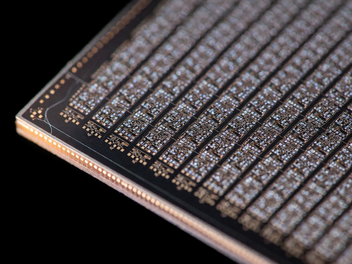
AMD’s MI350X carries 288 GB of HBM3E memory for large-scale AI workloads. This capacity is 50% higher than the 192 GB on the MI300X. The memory bandwidth reaches 8.0 TB/s, which is a significant increase over the 5.3 TB/s on the MI300X. The CDNA 4 architecture uses TSMC’s N3P 3nm process node for its compute dies and utilizes eight Accelerator Compute Dies stacked atop four base dies to reach 185 billion transistors. Each XCD contains 32 CDNA 4 Compute Units, giving the full accelerator 256 CUs. This design handles 400B+ parameter models using only three MI350X GPUs at FP16, whereas the NVIDIA B200 requires five GPUs for the same model. You know that fitting large models into VRAM often matters more than raw TFLOPS. AMD uses Infinity Fabric for multi-GPU scaling, which provides 1,075 GB/s of bidirectional aggregate bandwidth per socket. The MI355X variant uses liquid cooling to reach a 1,400W TBP, which provides a 20% performance advantage over the air-cooled MI350X. The MI350X provides 256 MB of Infinity Cache on the base dies. This cache includes 128 channels, each with 2 MB of capacity. The MI350X provides 72.1 TFLOPS of FP64 throughput, which is over double the 34 TFLOPS from the H100. This 2.1x advantage makes the MI350X a strong candidate for scientific and HPC workloads.
Compute density and precision types
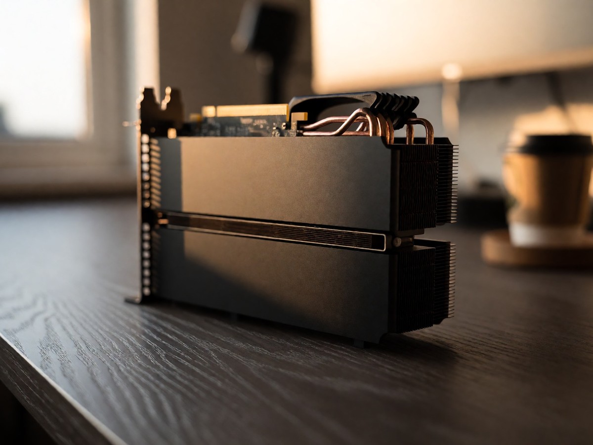
The MI350X delivers 4,614 TFLOPS of FP8 dense throughput. This figure is over twice the 1,979 TFLOPS provided by the NVIDIA H100. CDNA 4 includes native hardware support for MXFP4 and MXFP6 formats. These formats allow for aggressive quantization. The MI350P, a PCIe variant, carries 144 GB of HBM3E memory and has a 4.0 TB/s bandwidth. It has a 600W TBP, which is configurable down to 450W. The MI350P delivers 4,600 TFLOPS at MXFP4 precision. The MI350P contains 128 compute units, 512 matrix cores, and 8,192 stream processors running at 2.2 GHz. This PCIe card delivers 39% better FP8 performance and 43% better FP16 performance than the NVIDIA H200 NVL. The CDNA 4 architecture adds a new vector ALU to the Compute Unit. This ALU supports 2-bit operations and can accumulate BF16 results into FP32. The Local Data Share capacity is 160 KB per Compute Unit, which is an increase from the 64 KB in CDNA 3. This expanded capacity doubles the read bandwidth to 256 bytes per clock cycle.
| Specification | AMD MI350X | NVIDIA B200 | NVIDIA H100 |
|---|---|---|---|
| Memory Capacity | 288 GB | 192 GB | 80 GB |
| Memory Bandwidth | 8.0 TB/s | 8.0 TB/s | 2.0 TB/s |
| FP8 Dense Throughput | 4,614 TFLOPS | – | 1,513 TFLOPS |
| FP4 Dense Throughput | 9,227.5 TFLOPS | – | Not supported |
The MI350X provides 2,309.6 TFLOPS at FP16 precision. The H100 provides 989.5 TFLOPS at the same precision. The MI350X produces 2.2x more FP32 throughput than the H100.
Software and deployment economics
AMD’s ROCm 7.x supports PyTorch, JAX, vLLM, and SGLang. The software stack includes HIP for porting CUDA code. ROCm still trails CUDA 13.x in ecosystem depth. The MI350X provides a 33% lower hardware cost per token for FP8 deployments of large models compared to the B200. A Llama 4 Maverick deployment at FP16 requires 800 GB of memory. This model needs 3 MI350X GPUs but needs 5 B200 GPUs. This memory advantage creates a 40% lower hardware cost per token for FP16 workloads. The MI350P is a standard full-height, full-length, dual-slot PCIe card. It fits into off-the-shelf air-cooled servers. Companies like Dell, HPE, and Supermicro provide qualified servers for the MI350P. DigitalOcean lists MI350X at $6.16 per GPU-hour. Spheron lists the B200 at $4.42 per GPU-hour. Will the ROCm ecosystem catch up to CUDA’s maturity for specialized kernels? The MI350X is the better choice for large-parameter inference workloads where memory capacity dictates deployment scale.