
Lightmatter joined the NVIDIA NVLink Fusion ecosystem in June 2026. This partnership combines Lightmatter’s Passage CPO and NPO products with NVIDIA’s optical and SerDes technology. Lightmatter provides high-performance optical connectivity for AI infrastructure. I see Lightmatter’s focus on the chip-to-chip interconnect as the necessary correction to the industry’s reliance on electrical links. While NVIDIA scales through massive GPU clusters and rack-scale switches, Lightmatter addresses the internal communication bottleneck between chiplets. This combination suggests a hybrid future where optical links connect both individual dies and entire racks.
The Physical Limits of Copper Interconnects
You already know that electrical interconnects struggle as signaling rates climb. Copper traces hit physical boundaries when data rates reach 56 Gbps NRZ and above. Signal loss and RC delay increase with distance and frequency. These electrical limitations restrict the usable range of copper links to less than two meters in high-demand configurations. This creates a physical boundary for rack design. As AI accelerators demand more bandwidth, the energy needed to move each bit via copper rises. I observe that the industry must move toward optics to overcome these electrical constraints. The industry bottleneck is shifting from individual processor performance to the movement of data between processors.
Lightmatter’s Passage M1000 Photonic Interposer
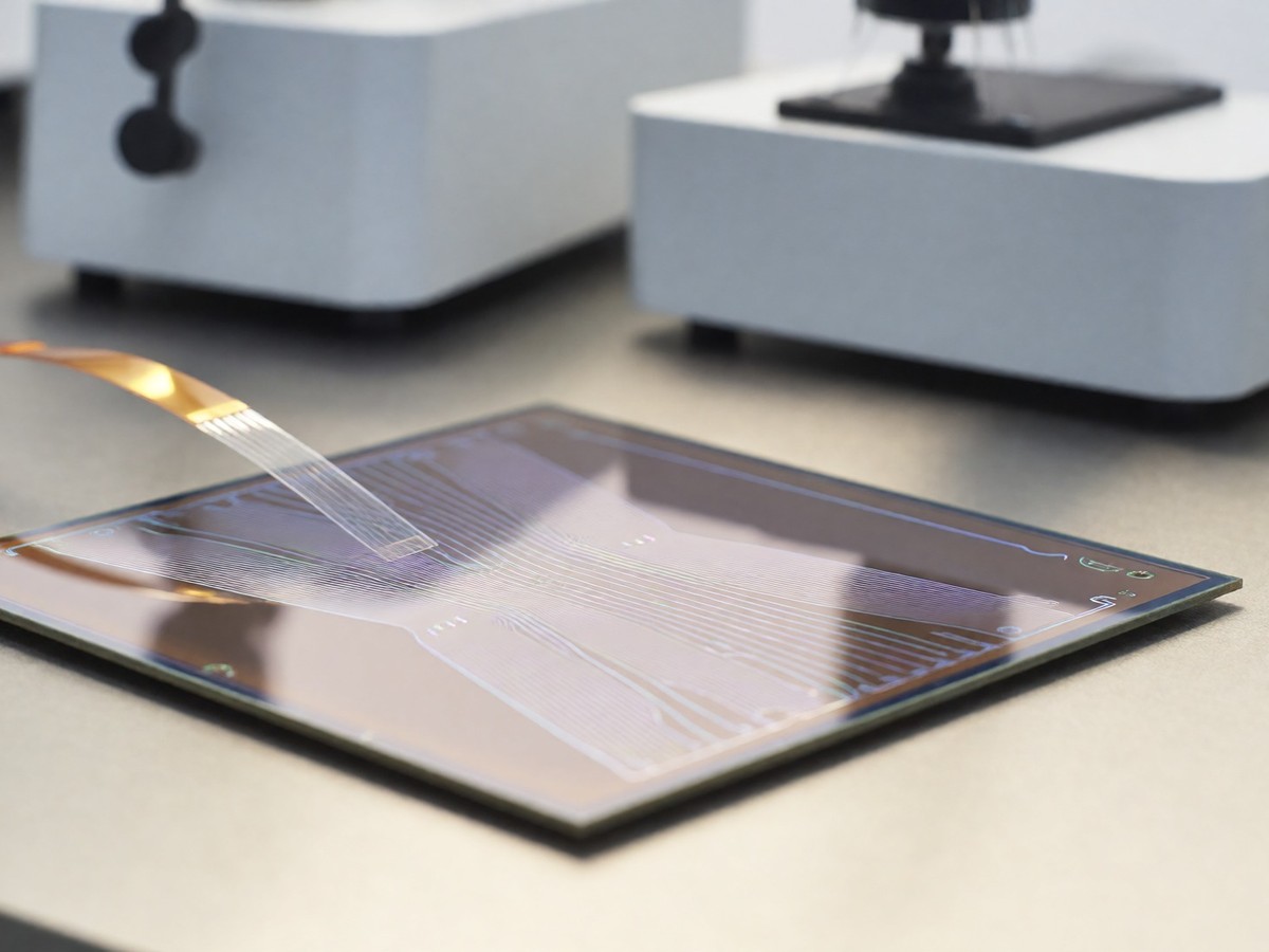
The Passage M1000 uses a 4,000 mm2 3D photonic interposer to replace electrical die-to-die connections with optical waveguides. This substrate integrates up to 34 chiplets. It provides 114 Tbps of total bidirectional bandwidth. The platform includes 1,024 high-speed SerDes lanes. It uses 8-wavelength WDM per fiber to multiply bandwidth without increasing fiber count. The M1000 replaces periphery-limited I/O pins on monolithic chips with multi-terabit-per-second I/O bandwidth. The 4,000 mm2 die size exceeds the traditional reticle limit of a single chip. This multi-reticle design introduces stitching defects at reticle boundaries and reduces yield relative to smaller dies. While NVIDIA focuses on increasing performance through massive GPU clusters and rack-scale optical switches, Lightmatter targets the internal communication between chiplets using a 3D photonic interposer that manages 114 Tbps of bidirectional bandwidth.
NVIDIA Blackwell and the Scaling Dilemma
The NVIDIA Blackwell B200 is the flagship GPU architecture. It contains 208 billion transistors across two TSMC 4NP dies. These dies connect via a custom 10 TB/s chip-to-chip interconnect. The B200 includes 192 GB of HBM3e memory with 8 TB/s bandwidth. It achieves 20 PFLOPS of peak FP4 performance. The B200 requires 1,000W of power and liquid cooling. The B300 variant increases memory to 288 GB and power to 1,100W. The GB200 Grace Blackwell Superchip pairs one Grace CPU and two Blackwell GPUs via NVLink-C2C at 900 GB/s. This connection is 7x faster than PCIe Gen 5. The GB200 NVL72 rack connects 72 Blackwell GPUs and 36 CPUs. It provides 1.8 TB/s per-GPU interconnect bandwidth. This architecture delivers 30x faster LLM inference than a comparable H100 cluster. The B200 delivers 9,000 TFLOPS of sparse FP8, which is 2.3x the performance of the H100 and H200.
The Passage L20 Optical Engine
The Passage L20 is a 6.4 Tbps optical engine for NPO and OBO applications. It supports 200 Gbps per lane DR data rates. The module uses 2-wavelength BiDi multiplexing. This technology reduces fiber management requirements by 50% compared to unidirectional DR standards. The L20 uses 224G PAM4 electrical signaling. It follows IEEE 802.3dj standards. The module has a 30W TDP and a 2000-pin BGA form factor. It provides 32 optical ports. The L20 enables drop-in compatibility for existing XPU and switch packages. This expansion of the Passage portfolio provides architectural flexibility for customers who need to choose an integration strategy for their XPU and switch roadmaps.
Comparing Scale-Up Strategies
Cerebras builds the WSE-3 with 4 trillion transistors and 900,000 sparse linear algebra cores. The WSE-3 integrates 42 GB of on-chip SRAM with 21 PB/s of memory bandwidth. A single Cerebras CS-3 system consumes up to 15 kW. Cerebras uses SwarmX to link thousands of WSEs. Graphcore’s Bow IPU uses TSMC’s Wafer-on-Wafer technology. It bonds a compute wafer with 1,472 AI cores to a passive power-delivery wafer. This design allows the IPU to run at 1.85 GHz. It provides a 40% performance boost and 16% energy efficiency improvement. Tachyum is developing the Prodigy chip with a multi-core design. Lightmatter’s Passage offers a different compromise by using optical interconnects to achieve giant-chip-like performance via dense optical links between smaller dies.
The Interconnect Standard Battle
NVIDIA controls the AI infrastructure through NVLink, NVSwitch, InfiniBand, and Spectrum-X. The Spectrum-X and Quantum-X switches integrate co-packaged optics. These switches provide 1.6 Tbps per port and improve energy efficiency. AMD, Broadcom, Meta, Microsoft, and OpenAI support open alternatives. UALink targets low-latency communication inside scale-up domains with 200 Gbps per lane. The UALink specification supports up to 1,024 accelerators in a computing pod. Broadcom’s Tomahhawk 5-Bailly platform integrates silicon photonics directly into the switch. Broadcom shipped 50,000 units of the Bailly platform in 2025. Marvell acquired Celestial AI for $3.25 billion in December 2025 to compete in the chip-to-chip optical layer.
The Economics of Optical Scaling
The transition to optics changes the economics of the data center. Networking consumes 20 percent of data center energy. Replacing copper with optics can release enough power to install another 1,000 GPUs. Market forecasts for Co-packaged Optics vary widely. Mordor Intelligence projects a $2 billion market by 2030. DigiTimes projects a $130 billion market by 2030. This difference stems from whether analysts include scale-out pluggables or only scale-up CPO. How will the manufacturing yield of these massive photonic interposers impact the total cost of ownership for hyperscalers?