The global photonic chip market is projected to expand from approximately $4 billion in 2025 to $9.3 billion by 2032, growing at a compound annual rate of 12.9%. This surge is driven by the physical limits of electrical interconnects, which cap bandwidth and spike power consumption in large AI clusters. I see optical interconnects as the largest application segment because they solve the "shoreline" constraint that restricts data movement to chip edges. North America currently holds the largest regional share, while thin-film lithium niobate emerges as the fastest-growing material platform. Silicon photonics retains the largest material share due to its compatibility with CMOS manufacturing, but the industry is shifting toward heterogeneous integration to support co-packaged optics architectures.
Breaking the Shoreline Constraint
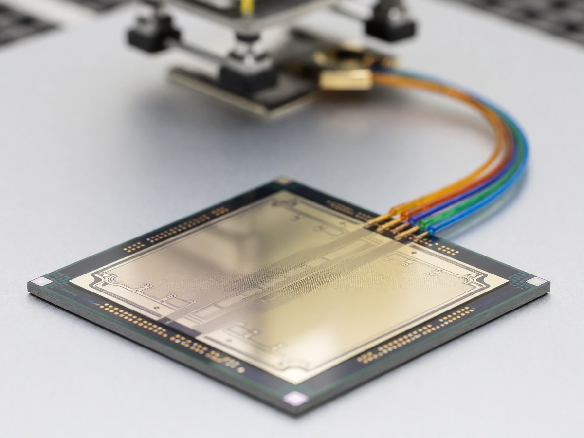
Lightmatter’s Passage M1000 is a 3D-stacked active photonic interposer designed to eliminate the edge-limited I/O bottleneck. It delivers 114 Tbps of total optical bandwidth across a 7,735 mm2 package that supports up to 1,500W of power delivery. The device uses eight connected chip sections in one package, integrating 1,024 serial data channels each supporting 56 Gbps transmission. For external connections, it incorporates 256 fiber-optic lines with eight wavelengths per signal line, each offering 448 Gbps. Unlike conventional designs where signals route around the perimeter, the M1000 embeds optical waveguides throughout the entire surface, enabling "edgeless connectivity" for compute tiles stacked directly on top. This vertical stacking reduces latency and signal degradation compared to longer electrical paths. Lightmatter claims this design can reduce power consumption by 10x to 100x relative to conventional GPUs, a figure that sounds aggressive but aligns with the physics of optical signaling at high data rates.
The manufacturing ecosystem behind the M1000 relies on GlobalFoundries’ Fotonix silicon photonics platform, which integrates lasers, modulators, and CMOS logic on a single wafer. Packaging partners Amkor and ASE handle the complex alignment of optical waveguides and dense fiber arrays required for volume production. While the technology promises significant efficiency gains, the transition from module-level assembly to wafer-level heterogeneous integration presents substantial engineering hurdles. Precision alignment and thermal management for chips dissipating kilowatts of heat remain difficult to scale reliably. Standardization efforts by organizations like the Optical Internetworking Forum are still developing common electrical specifications between switch ASICs and optical engines, which may slow widespread adoption despite the clear performance benefits.
Co-Packaged Optics and Market Momentum
Co-Packaged Optics (CPO) is moving from an emerging concept to core infrastructure as commercial switch deployments begin in 2026. Ayar Labs partnered with Alchip Technologies and TSMC to integrate optical I/O into high-performance ASICs, addressing the need for multi-rack scale-up systems. Their TeraPHY chiplet enables optical I/O bandwidth exceeding 1 Terabit/sec at 10 times lower power than current Gigabit/sec solutions. This approach removes the limitations of copper interconnects, allowing for extended memory and computing resources across larger data centers without proportional increases in energy use.
Investor confidence in these technologies is evident in recent funding rounds. Celestial AI raised $250 million in Series C1 funding led by Fidelity Management & Research Company for its photonic fabric technology. Meanwhile, Ayar Labs secured $155 million in Series D funding led by Advent Global Opportunities and Light Street Capital. These capital injections support the development of specialized inference accelerators, which analysts predict will grow faster than training workloads. The shift toward photonic solutions is not just about speed; it is about sustaining the operational costs of hyperscale AI infrastructure. As models become more complex, the energy burden of moving data becomes a primary cost driver. I question whether the current supply chain can handle the precision requirements for mass production of these advanced packages, but the financial backing suggests the industry believes the answer is yes. The race to integrate light-based processing is no longer theoretical; it is a competitive reality defined by specific terabits per second and wattage limits.