
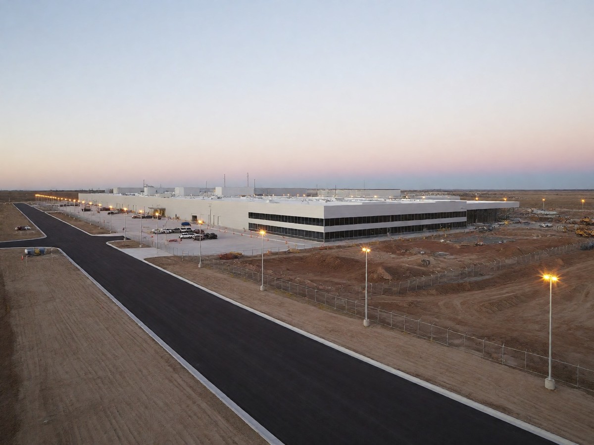
Samsung Electronics’ foundry division manufactures Tenstorrent’s next-generation RISC-V AI chiplets using the SF4X 4nm process. This partnership targets data center and automotive industries. Samsung’s manufacturing expansion in Taylor, Texas, provides the capacity for these advanced chiplets. Tenstorrent selected Samsung’s Foundry Design Service team because of their expertise in silicon manufacturing. Jim Keller, the Tenstorrent CEO, says Samsung’s semiconductor technology aligns with Tenstorrent’s vision for RISC-V and AI. Tenstorrent also recently closed a Series D funding round of over $693M. Samsung Securities and AFW Partners led this oversubscribed round. The company reached a pre-money valuation of $2B. Other investors include Hyundai Motor Group, Fidelity Management & Research Company, and Bezos Expeditions.
The evolution from Jawbridge to Wormhole
Tenstorrent’s hardware evolution began with the Jawbridge testchip, a proof-of-concept design. This small chip validated power and performance claims with a minimal budget. GraySkull followed as the first commercial product, utilizing the GlobalFoundries 12nm process. GraySkull shipped A0 silicon with no erratum on its first tapeout. This chip contained 128 Tensix cores on a 620mm2 die. Wormhole uses the same 12nm process but grows the die to 670mm2. Wormhole scales performance and IO while only doubling the power to 150W. It also adds 16 ports with 100Gb Ethernet to allow chips to link for large AI networks. Jim Keller, who previously worked at AMD, Apple, Intel, and Tesla, leads the design philosophy at Tenstorrent. This design focuses on an open ISA and a compiler stack built as an open-source project.
Tensix architecture and data movement
The Tensix core functions as a self-contained compute tile. It contains three parts: a RISC-V data movement processor, an 8×8 BF16 tile multiply-accumulate unit, and a vector unit for element-wise operations. The vector unit handles element-wise operations such as activations and normalizations. The matrix engine performs 8×8 BF16 tile multiply-accumulate operations. The RISC-V processor manages memory operations and kernel control flow. Each Tensix core holds 1.5 MB of local L1 SRAM. The n300 card has 128 Tensix cores across both ASICs, providing 192 MB of on-chip SRAM in aggregate. The architecture requires explicit data movement. The programmer or compiler schedules when data moves from DRAM to SRAM and when it moves back. There is no hardware prefetcher to guess access patterns. This makes performance predictable when the programmer gets it right, but debugging becomes painful when they do not.
Memory hierarchy and NVIDIA comparisons
I find the memory hierarchy a major difference between Tenstorrent and NVIDIA. The n300 card has 24 GB of GDDR6 with 576 GB/s bandwidth. An NVIDIA H100 SXM5 has 80 GB of HBM3 with 3.35 TB/s bandwidth. This 6x bandwidth gap creates a bottleneck for large-batch inference with large KV caches. However, the 192 MB of aggregate on-chip SRAM helps when the working set fits in SRAM. Small-batch inference remains more favorable for the n300 due to this trade-off. You already know that NVIDIA dominates the inference market with its proprietary software stack. The n300 provides 466 TFLOPS in FP8, while the H100 provides 1,513 TFLOPS in FP8. The n300 provides 131 TFLOPS in FP16, while the H100 provides 102.4 TFLOPS in FP16. The n300 provides 262 TFLOPS in Block FP8. The n300 card costs $1400, whereas the H100 is priced north of $30,000.
Wormhole PCIe card specifications
| Specification | n150d | n150s | n300d | n300s |
|---|---|---|---|---|
| Wormhole ASICs | 1 | 1 | 2 | 2 |
| Tensix Cores | 72 | 72 | 128 | 128 |
| AI Clock | 1 GHz | 1 GHz | 1 GHz | 1 GHz |
| SRAM | 108 MB | 108 MB | 192 MB | 192 MB |
| Memory | 12 GB GDDR6 | 12 GB GDGD6 | 24 GB GDDR6 | 24 GB GDDR6 |
| Memory Bandwidth | 288 GB/s | 288 GB/s | 576 GB/s | 576 GB/s |
| TeraFLOPS (FP8) | 262 | 262 | 466 | 466 |
| TeraFLOPS (FP16) | 74 | 74 | 131 | 131 |
| TBP (Total Board Power) | 160W | 160W | 300W | 300W |
| Connectivity | 2x Warp 100 Bridge | 2x Warp 100 Bridge | 2x Warp 100 Bridge | 2x Warp 100 Bridge |
Scaling via Nebula and Galaxy systems
Scaling requires the Nebula 4U server chassis, which houses 32 Wormhole chips. These chips connect in a full mesh internally. The Galaxy rack connects 8 Nebulas in an extended mesh. The Galaxy rack includes 4 AMD Epyc servers and a shared memory pool. It provides over 3 TB of GDDR6 and 256 Gb of external Ethernet links. The 32 Wormhole processors in a Galaxy board connect through an on-chip Ethernet mesh without a PCIe switch. When users plug multiple n300 cards into a Galaxy board, the Ethernet fabric connects the chips, allowing the 32 Wormhole processors to form a 2D mesh where each node reaches any other node through these links. Tenstorrent supports multiple topologies, including the leaf and spine models common in datacenters. The on-chip network scales up transparently to many racks without rewriting software. Historically, scaling across CPU clusters required large batch sizes and parameter servers to aggregate batches. GPU clusters using all-reduce and higher bandwidth between nodes led to further advancements. However, researchers eventually hit a limit with batch sizes because large batches can prevent model convergence.
The Blackhole architecture
Blackhole succeeds Wormhole as the next-generation architecture. The p100 card uses a single Blackhole die with 120 Tensix compute cores. It adds 16 big RISC-V cores, organized in 4 clusters of 4. These cores manage data movement on-die, which reduces host CPU overhead for small-batch workloads. The p150 developer card costs $1,399 and provides 32 GB of GDDR6. It draws up to 300W in the active-cooled workstation form factor. Tenstorrent reduced the p150 core count from 140 to 120 because disabling 20 cores on the 600mm2 die improved yields. This reduction means any benchmark published before the change might not match current performance. Blackhole also provides native PCIe 5.0 support, which maintains backward compatibility with existing CUDA servers. This allows teams to slot Blackhole cards into the same PCIe infrastructure used for NVIDIA GPUs.
Software maturity and the final verdict
Tenstorrent uses the open-source TT-Metal compiler stack. This software contains 50,000 lines of code. It is MIT-licensed and available on GitHub. Users can read every kernel and modify allocation decisions. This differs from NVIDIA’s CUDA, which relies on proprietary software like cuDNN and cuBLAS. The n300 provides 350 t/s on Mistral-7B at a batch size of 32. In contrast, the H100 performs significantly higher. I recommend Tenstorrent for sovereign AI programs or hardware research groups that require a fully auditable, open-ISA stack. The open-source nature of the compiler provides an alternative for users who require an auditable compute stack for regulated workloads. Can Tenstorrent’s software stack catch up to NVIDIA’s ecosystem before the market shifts entirely to specialized ASICs?