The August 2025 Dojo shutdown
Musk disbanded the Dojo team and shut down the project in August 2025. This decision followed his statement that Dojo 2, the second supercluster intended to use D2 chips, constitutes an evolutionary dead end. Tesla’s shift toward the AI6 chip, which scales from FSD to Optimus, drove this change. The company also expects AI6 to support large-scale AI training.
The shutdown followed several months of speculation regarding the future of Tesla’s custom hardware. In July 2025, Musk stated that Dojo 2 would operate at scale sometime in 2026. However, he later declared that once it became clear that all paths converged to AI6, he had to shut down Dojo and make tough personnel choices because the Dojo 2 project had become an evolutionary dead end.
This decision resulted in significant personnel changes within the AI division. Peter Bannon, the lead for Dojo, left the company. Around 20 other workers also departed to form DensityAI, a startup focused on AI chips and infrastructure. These departures occurred alongside the announcement of a $16.5 billion deal with Samsung to secure next-generation AI6 chips.
The change in strategy follows a period where Tesla shifted its focus toward the Cortex cluster in Austin. Cortex uses 50,000 Nvidia H100 GPUs to power FSD training. While Dojo was intended to reduce reliance on Nvidia, the company continues to use Nvidia hardware for its superclusters. Does the shift toward the AI6 architecture negate the necessity of the original Dojo 2 roadmap?
Technical specifications of the D1 architecture
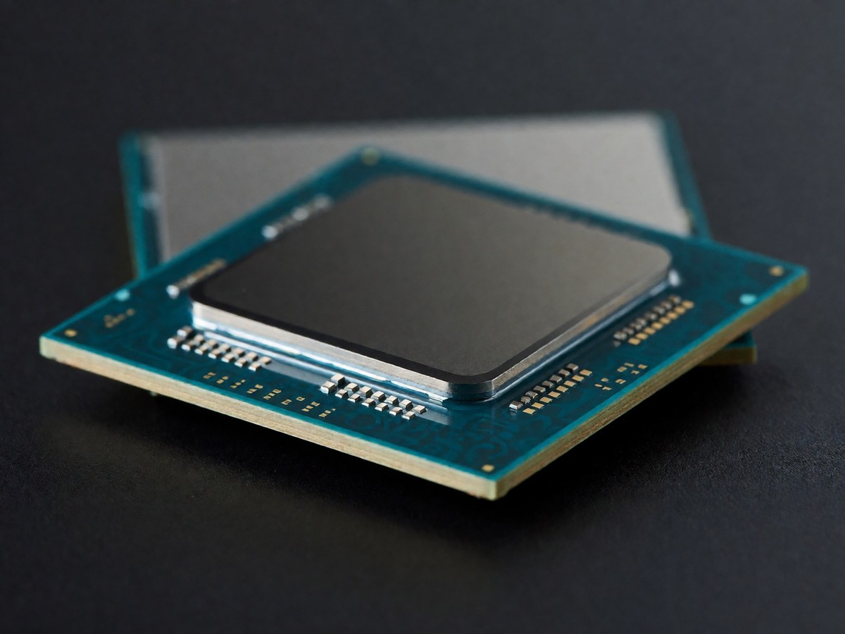
The D1 chip contains 50 billion transistors and uses a 7 nanometer process. Each die covers 645 square millimeters. A single chip provides 354 computing cores for applications. These cores run at 2 gigahertz. Every core has 1.25 megabytes of SRAM main memory. The total SRAM on the die equals 440 megabytes. The chip achieves 376 teraflops when using 16-bit brain floating point numbers or configurable 8-bit floating point numbers. It reaches 22 teraflops at FP32 precision.
The architecture uses a 2D mesh network to link cores. A 32-byte fetch window holds up to eight instructions per node. The chip utilizes a 4-wide, 4-way SMT scalar scheduler. A dedicated vector scheduler feeds either a 64-byte SIMD unit or four 8x8x4 matrix multiplication units. The 2D mesh network allows a single packet to go in and out in all four directions to and from each neighbor node. Each chip also includes 576 bi-directional serializer/deserializer channels along the perimeter. These channels move 8 terabytes per second across all four die edges.
A single training tile packages 25 D1 chips in a 5×5 array. Each tile consumes 15 kilowatts of power. The tile supports 36 terabytes per second of aggregate bandwidth via 40 input/output chips. It also provides 10 terabytes per second of on-tile bandwidth. A single tile achieves 9 petaflops at BF16 or CFloat8 precision. These tiles aggregate into System Trays, which contain six tiles and 53,100 D1 cores.
The transition to AI5 and AI6 systems
Tesla produces different chips to manage the various requirements of its AI ecosystem. AI5 serves as the high-performance inference successor to the current HW4 hardware. It uses a dual-fab strategy to ensure supply. Tesla manufactures AI5 chips at Samsung Taylor in Texas and at TSMC Arizona. This strategy avoids the single-point-of-failure risks seen in previous chip shortages.
AI6 represents the next generation of low-power chips designed for the Cybercab robotaxi and Optimus humanoid robots. AI6 optimizes inference efficiency per watt to fit within the thermal limits of compact vehicle architectures. Using AI5 in a robotaxi would require thermal management systems that consume too much vehicle volume and battery capacity. AI6 avoids this by providing high inference capability at a lower thermal design power.
You already know the basics of Tesla’s shift toward custom silicon. The company aims for a 9-month design cycle for these next-generation chips. The AI6 chip is expected to tape out by December 2026. Mass production for AI6 will begin in the second half of 2027. Adoption of these chips in vehicles and robots will follow in 2028.
The company views the convergence of training and inference as a way to simplify its hardware stack. Musk noted that putting many AI5 or AI6 chips on a single board reduces network cabling complexity and cost. This approach effectively creates what he calls Dojo 3. The AI6 design facilitates this by scaling from onboard inference to large-scale data center training.
Three-tier semiconductor manufacturing strategy
Tesla employs a three-tier semiconductor manufacturing architecture to manage supply risks. The first tier involves a captive-equivalent dedicated line at Samsung Taylor in Texas. This arrangement uses a 10-year exclusive supply agreement for AI5 production. Tesla engineers have on-premise access to the production line to participate in yield improvement programs. This allows for a continuous process improvement loop that functions as the operational equivalent of owning a fab without carrying the capital on the balance sheet.
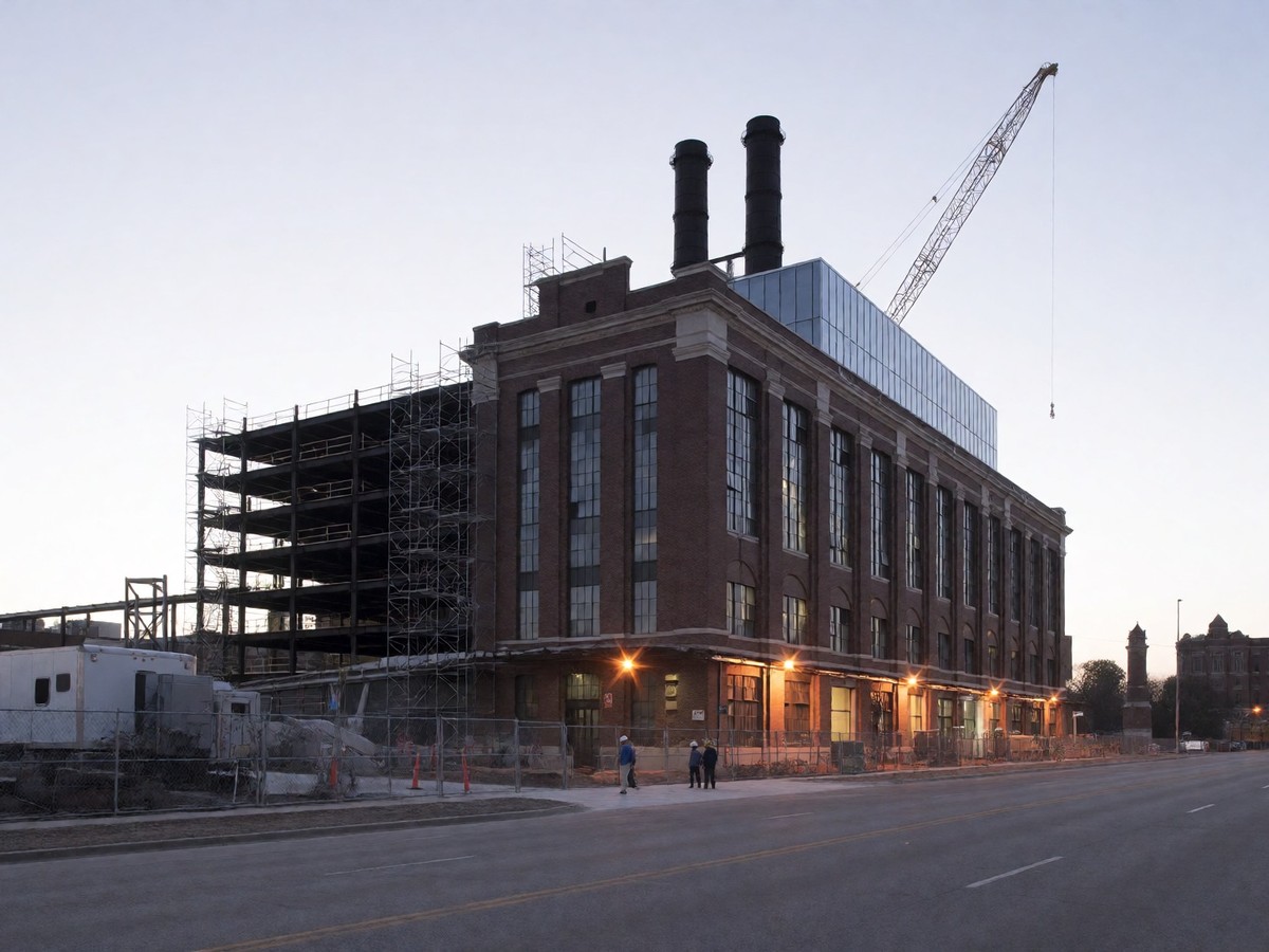
The second tier uses a shared external foundry relationship at TSMC Arizona to provide supply resilience for AI5. This prevents production halts if one foundry faces disruption. The third tier consists of Terafab, a joint venture between Tesla, SpaceX, and xAI. Terafab serves as the owned production base for AI6 and AI7 chips. This project began in March 2026 at the Seaholm Power Plant site in Austin, Texas.
Terafab requires $20 billion to $25 billion in capital and a 5-7 year buildout period. It uses a 2nm process to produce chips for ground-based deployment. The facility manages the production of AI6 for robots and AI7 for orbital computing. This vertical integration seeks to control the supply chain from design to manufacturing.
| Training Hardware Component | Tesla Dojo ExaPOD | NVIDIA Training Cluster |
|---|---|---|
| Primary Processor | Custom D1 chips | NVIDIA H100/H200 GPUs |
| Fabrication Node | 7nm (D1) | Various |
| Interconnect Method | 2D Mesh Network | NVLink and InfiniBand |
| Memory Configuration | 1.25MB SRAM per core | High-bandwidth memory (HBM) |
| Scaling Architecture | Training Tiles/ExaPODs | Modular GPU nodes |
The D1 chip remains the primary driver for the Dojo training project. It provides high bandwidth and low latency for video processing. This differs from the modular expansion used in NVIDIA-based GPU clusters.
Comparing custom silicon to NVIDIA hardware
Tesla utilizes a hybrid approach to AI training. It uses custom Dojo hardware and large-scale NVIDIA GPU clusters. The company deployed 10,000 NVIDIA H100 GPUs in a new training cluster. It also maintains a cluster in Austin consisting of 50,000 H100 GPUs. These NVIDIA clusters handle diverse workloads that require high flexibility.
The custom Dojo architecture targets specific efficiency gains for video AI training. The D1 chip focuses on the unique needs of Full Self-Driving neural networks. This specialization aims to increase bandwidth and decrease latencies compared to general-purpose GPUs. However, Tesla still faces competition from NVIDIA and AMD in the training market.
Managing the data from 160 billion frames of video per day remains a significant challenge. Large-scale training requires massive storage and high-speed interconnects. The NVIDIA hardware provides a mature ecosystem for these tasks. Tesla’s strategy relies on combining this established ecosystem with its own specialized silicon.
The cost of AI training is a major factor in the decision to build custom chips. Tesla invested $500 million to build a Dojo supercomputer in Buffalo. The company also plans to spend over $1 billion on Dojo through 2024. The shift toward AI6 and AI7 represents a move to control these costs through internal production.
The 2026 Dojo restart and Terafab project
The Dojo project did not end permanently in 2025. Tesla restarted work on Dojo 3 in January 2026. This restart follows progress made on the design of the AI5 chip. The new iteration of Dojo focuses on large-scale AI training using the latest chip designs.
The Terafab project launched in March 2026 in Austin. This joint venture between Tesla and SpaceX aims to build a massive chip production base. Terafab supports the production of AI6 and AI7 chips. The project uses a 2nm process to meet the requirements of future autonomous systems.
Tesla manages multiple computing clusters to develop Autopilot. The primary unnamed cluster uses 5,760 Nvidia A100 GPUs. This cluster reached approximately 81.6 petaflops in 2021. Tesla also operates a second cluster with 4,032 GPUs for training. A third cluster contains 1,752 GPUs for automatic object labeling.
The development of Terafab coincides with the rollout of the AI6 chip. This chip supports the needs of both the Cybercab and the Optimus robot. The project emphasizes scaling production to meet the needs of 100 million Optimus units. The Austin facility serves as the center for this advanced manufacturing effort.
Manufacturing the AI7 for orbital compute
The AI7 chip is designed specifically for SpaceX orbital computing. This chip serves the Starlink constellation and future satellite platforms. AI7 requires low power and radiation tolerance to function in low Earth orbit. This specification addresses the threat of total ionizing dose and single-event upsets.
AI7 uses a 2nm process developed at the Terafab facility. This process is shared with the AI6 chip but includes specific modifications. Tesla and SpaceX engineers control the process parameter space to ensure reliability. This level of control is necessary because commercial foundries do not develop specialized radiation-tolerant processes for single customers at satellite volumes.
The demand for AI7 scales with the growth of the Starlink constellation. The constellation grows from thousands to tens of thousands of satellites. This creates a sustained high-volume demand for specialized orbital compute. The production of AI7 remains a primary driver for the Terafab investment.
The production of AI7 requires a specialized set of mitigation techniques. These include hardened cell libraries and error-correcting code on all memory. The design also uses triple modular redundancy on safety-critical control paths. These features ensure the chip survives the environment of low Earth orbit.
Redefining the training roadmap
Tesla’s training roadmap focuses on the convergence of hardware and software. The company designs its chips to run its specific neural network architectures. This allows for higher efficiency than using general-purpose hardware. The move toward AI6 and AI7 demonstrates this long-term plan.
The company expects the AI6 chip to provide the necessary performance for both the Cybercab and Optimus. AI6 focuses on maximizing inference efficiency per watt. This efficiency is vital for the battery capacity constraints of humanoid robots. The design of AI6 is a departure from the high-power approach of AI5.
The timeline for these developments remains aggressive. AI5 reaches high-volume production in 2027. AI6 follows in the second half of 2027. The company targets a 9-month design cycle for all subsequent generations. This rapid iteration helps Tesla keep pace with the advancing requirements of autonomous driving.
The deployment of AI6 in vehicles and robots will happen in 2028. This rollout depends on the successful scaling of the 2nm process at Terafab. Tesla continues to refine its training algorithms to match the capabilities of its new silicon. The strategy relies on tight integration between the chip design and the software stack.