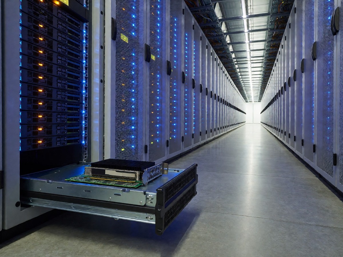
Google engineers calculated that if every Android user used voice search for just three minutes a day, the company would need to double its entire data center capacity to handle the massive increase in neural network inference requests. This 2013 projection drove the recruitment of Amir Salek to establish custom silicon development capabilities for Google’s data centers. Norm Jouppi led the design, verification, and deployment of the first TPU in just 15 months. The first-generation TPU used a 28nm process and consumed 40W when running. It delivered 92 trillion 8-bit operations per second through its 256×256 systolic array. This hardware fits into a SATA hard disk slot via a PCIe Gen3 x16 bus that provides 12.5GB/s of effective bandwidth. The TPU v1 focused on inference and silently accelerated services like Google Maps, Google Photos, and Google Translate. This initial deployment demonstrated that specialized hardware could achieve 15 to 30 times higher performance and 30 to 80 times higher performance-per-watt than contemporary CPUs and GPUs.
Evolution of the systolic array
The TPU architecture uses a systolic array to handle tensor math. In this design, data flows through a grid of multiply-accumulate units. This movement reduces the need for complex control logic and minimizes data movement energy costs. The TPU v1 featured 65,536 8-bit multiply-and-add units. This design allowed the TPU to power the AlphaGo series that defeated Lee Sedol. The 2016 AlphaGo victory proved that specialized silicon, rather than general-purpose processors, defines the ceiling of AI capability. In a systolic array, data enters the array once and flows through the grid, which eliminates constant memory access. You should know that these specialized chips target specific math patterns rather than general-purpose tasks. Since 2015, the TPU has evolved through several distinct stages. The 2017 TPU v2 introduced bfloat16 floating-point units and the first TPU Pod cluster using 2D ring interconnects. The 2018 TPU v3 added liquid cooling and expanded Pod clusters to 1024 chips. The 2021 TPU v4 utilized a 3D torus topology and 7nm process, which enabled a 4096-chip Pod. The 2023 TPU v5 series introduced the cost-optimized v5e and the high-performance v5p, which delivers 2.8x faster LLM training than v4. The 2024 Trillium architecture redesigned the system around inference, offering 4.7 times the performance of TPU v5e via larger matrix multiply units and increased clock speeds. The 2025 Ironwood architecture reached 4,614 TFLOPS of peak FP8 computing power and introduced 192GB of HBM3E memory with 7.37 TB/s of bandwidth. Each generation expanded the Matrix Multiply Engine, moving from 128×128 units in TPU v2 to 512×512 units in Ironwood.
The bifurcation of training and inference
The TPU lineup now splits into two distinct architectures for training and inference. The TPU 8t, designed by Broadcom, targets large-scale model pre-training. It delivers 12.6 FP4 PFLOPS of peak performance and includes 216 GB of HBM3e memory with 6,528 GB/s bandwidth. A single superpod of 9,600 chips delivers 121 FP4 ExaFLOPS of compute performance through the Virgo Network fabric. The TPU 8i, designed by MediaTek, targets low-latency serving and agentic workloads. It delivers 10.1 FP4 PFLOPS of peak performance and 288 GB of HBM3e memory. The 8i uses a Boardfly topology to reduce the maximum number of network hops from 16 to 7. It also uses a Collectives Acceleration Engine to cut collective communication latency by 5x. Migrating a PyTorch workflow to these TPUs means debugging compilation traces and restructuring loops. While the TPU 8t reaches 12.6 PFLOPS, it remains lower in peak performance than the NVIDIA GB200 or GB300. The 8i also contains 384 MB of on-chip SRAM, which is three times the amount found in Ironwood. The 8i provides 80% better performance-per-dollar than Ironwood for inference. Will these specialized architectures eventually displace the versatility of the GPU?
| Specification | TPU 8t (Training) | TPU 8i (Inference) |
|---|---|---|
| Peak Performance | 12.6 FP4 PFLOPS | 10.1 FP4 PFLOPS |
| HBM Memory | 216 GB HBM3e | 288 GB HBM3e |
| Memory Bandwidth | 6,528 GB/s | 8,601 GB/s |
| On-chip SRAM | 128 MB | 384 MB |
| Design Lead | Broadcom | MediaTek |