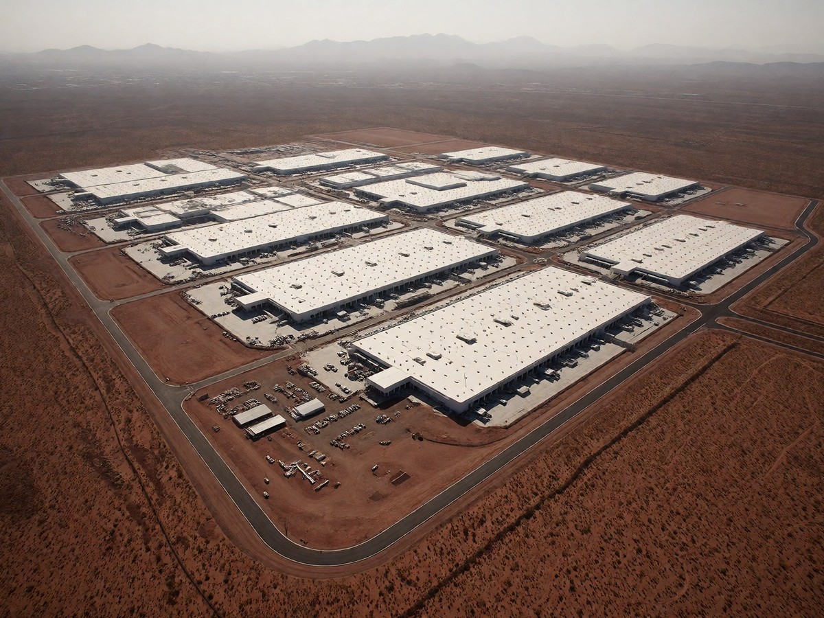
The temperature in the europe-west4-a data hall reached 44°C on July 15, 2026. This thermal excursion forced the immediate shutdown of Google Cloud VMware Engine, Bare Metal Solution, and Google Cloud NetApp Volumes. The disruption lasted for 14 hours and 55 minutes. A 3ms voltage transient in the utility power feed initiated the sequence of failures. While the side B Diesel Rotary Uninterruptible Power Supply (DRUPS) successfully took the load, the side A DRUSPs failed because of electrical component failures. This meant Row 3 lost both redundant power feeds and experienced a complete power loss. The incident impacted 24 private clouds belonging to 20 distinct customers.
The cooling failure happened because the chiller controller dropped offline during the voltage transient. This drop prevented the controller from signaling the chilled water distribution pumps to restart. Chiller system A shut down as a result. The facility lacked a redundant source because of ongoing construction work at the site. Engineers had to manually switch the pumps from auto to hand mode to restore water circulation. You should know that a loss of controller power can disable an entire data hall if the redundant systems also fail. I found the sudden loss of a chiller controller during a power event to be a massive vulnerability for high-density compute.
The voltage transient caused a load deployment discrepancy in the power feed. This discrepancy led to an overload protection breaker trip on the third row. Because the side A DRUPS could not take over the load, the facility experienced a complete power loss in that specific row. During the event, the server data hall experienced an increased temperature because the cooling system failed. The chiller controller dropped offline and failed to signal the chilled water distribution pumps to restart. This prevented the facility from maintaining safe temperatures. Google engineering teams initiated machine shutdown procedures for the remaining reachable devices as part of the cooling emergency shutdown process.
The mechanics of liquid cooling in the data center
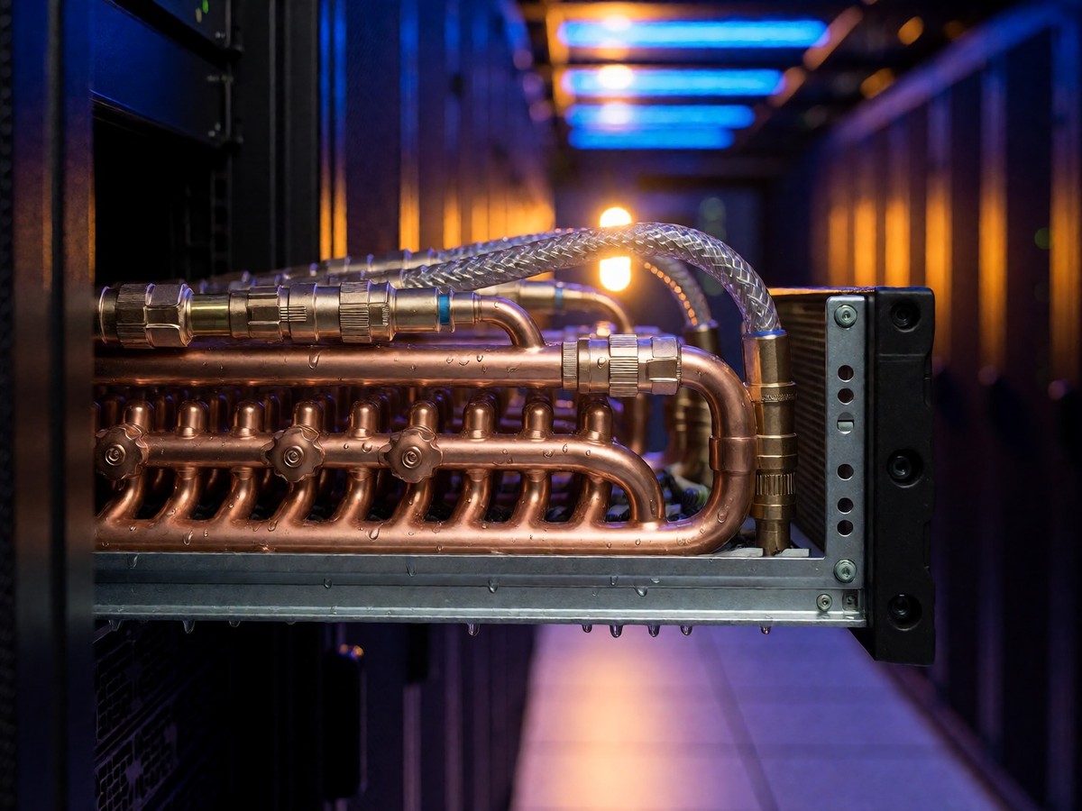
Google uses liquid cooling to handle the intense heat of AI accelerators. Water has a thermal conductivity about 4000 times greater than air. The architecture relies on Coolant Distribution Units (CDUs) to move heat between the coolant liquid and the facility water supply. These CDUs use flexible hoses and quick disconnect couplings to simplify maintenance. A single CDU rack provides enough capacity with five active units. The liquid moves from the CDUs through manifolds to the TPU servers. TPU chips connect in series within the loop. This design means some chips receive hotter liquid because it has already passed other chips in the loop.
Google uses a split-flow cold plate which performs better than a traditional straight-through configuration. The CDUs exchange heat between the coolant liquid and the facility-level water supply. These two liquid supplies do not mix, and the CDUs only move heat between the two pools of liquid. Cooling capacity depends on the requirements of the last chip in each loop. Maintenance of these systems requires high reliability because a small problem with one machine translates to a maintenance nightmare at scale. Google uses alerting systems to discover leaks and takes preventative measures like scheduled maintenance and filtration.
The industry is seeing a trend where liquid cooling is necessary due to increasing power draw and heat output. In enthusiast circles, there is a discussion about the efficiency of water-to-water heat exchange. Most mainframes have used water-to-water exchange for decades. Google uses huge chillers to cool water which is then directly pumped into every server. This eliminates air-based transfer except at the chiller tower. However, not all components can use liquid cooling. Passive components like resistors and FETs often require forced air because they lack a surface for a water block. The TPU sleds seem to address this by having an air-cooled portion for ancillary components.
Thermal management for the TPU v5p
The TPU v5p manages massive workloads with high density. A single TPU v5p Pod contains 8960 chips. Each chip delivers 459 TFLOPs of peak compute for BF16 and FP8 formats. The High Bandwidth Memory (HBM) capacity per chip is 95 GiB. This chip provides 2765 GBps of HBM bandwidth and 1200 GBps of bidirectional inter-chip interconnect (ICI) bandwidth. Developers can scale to 18432 chips using Multislice software. The maximum supported shape for a v5p Pod is a 16x16x24 configuration of 6144 chips. The TPU v5p uses a 3D torus topology with reconfigurable high-speed links that allow developers to connect chips in same-sized slices in multiple ways for demanding AI workloads.
The interconnect bandwidth per chip reaches 1200 GBps. The data center network (DCN) bandwidth per chip is 50 Gbps. Twisted torus topologies provide significantly higher bisection bandwidth for certain workloads. For example, a 4x4x8 twisted topology provides a 70% theoretical increase in bisection bandwidth compared to a non-twisted 4x4x8 slice. This increased bandwidth helps workloads that use global communication patterns. Twisted topologies change an asymmetric torus topology into a symmetric one. This provides improved load balancing, higher bisection bandwidth, and shorter packet routes.
The architecture relies on complex networking to maintain performance. A 4x4x2 torus topology provides different connectivity than a 16x16x24 shape. TPU software supports twisted topologies on slices where each dimension is either equal to or twice the size of the smallest dimension. This includes shapes like 4x4x8, 4x8x8, or 12x12x24. The ICI resiliency helps improve fault tolerance of optical links and optical circuit switches (OCS) between cubes. This resiliency allows ICI connections to be routed around OCS and optical ICI faults. It improves scheduling availability with the trade-off of temporary degradation in ICI performance.
The evolution of TPU architecture
The TPU lineage started in 2015 with TPU v1. This chip addressed the need for neural network inference without doubling the datacenter footprint. It featured a 256×256 systolic array of 8-bit integer units and delivered 92 teraops per second at 28 to 40 watts. TPU v2 arrived in 2017 and introduced training support via the bfloat16 format. This version increased memory bandwidth to 600GB/s and performance to 45 teraflops. TPU v3 brought liquid cooling to the architecture in 2018. This generation delivered 420 teraflops per chip and scaled to 2,048-chip pods.
TPU v4 introduced optical circuit switching in 2021. This technology uses MEMS mirrors to redirect light beams and patch TPU pairs together in sub-10-nanosecond windows. TPU v4 also included SparseCore to handle embedding operations for recommendation systems. The architecture includes four 128×128 MXUs per TensorCore. The TPU v5 generation split into TPU v5p for training and TPU v5e for cost-effective inference. TPU v5p achieves 4.45 exaflops per second across 8,960-chip pods. The Trillium generation, or TPU v6e, offers a 4.7x performance increase and 3x more inference throughput.
The latest developments focus on the age of inference. Ironwood, the seventh generation, is the first designed specifically for this phase. The Ironwood TPU delivers 4614 TFLOP/s and features 288 GB of HBM3e memory with 8601 GB/s of bandwidth. The chip also includes 384 MB of on-chip SRAM. The eighth generation, announced in April 2026, includes the TPU 8t and TPU 8i. The TPU 8t is optimized for large-scale pre-training and delivers 12.6 FP4 PFLOPs. It uses the Virgo Network fabric to scale up to 9,600 chips per superpod. The TPU 8i focuses on high-speed serving and delivers 10.1 FP4 PFLOPs with 384 MB of on-chip SRAM.
Scaling AI workloads with v5e and Trillium
The TPU v5e focuses on cost efficiency for smaller workloads. Eight TPU v5e chips cost approximately $11 per hour. This setup generates 2175 tokens per second on Llama2-70B. The v5e is optimized for models up to 200 billion parameters. It provides 3x more inference throughput per dollar than the previous generation. Google uses techniques like continuous batching via the JetStream library to maximize this throughput. This method can introduce a small queuing delay for each request.
The Trillium generation, or TPU v6e, offers significant improvements over its predecessors. It provides a 4.7x increase in peak compute performance per chip. Trillium also provides a 67% increase in energy efficiency and doubles the HBM capacity. It offers 3x more inference throughput than previous generations. Trillium provides up to 2.1x increase in performance per dollar over TPU v5e and up to 2.5x increase in performance per dollar over TPU v5p in training dense LLMs like Llama2-70b and Llama3.1-405b.
Training and serving fungibility allows users to use the same Cloud TPU quota for both tasks. Developers can scale to tens of thousands of chips to support demanding AI workloads. The GKE integration enables seamless AI workload orchestration using Google Compute Engine MIGs. This includes XPK for faster iterative development. The system manages TPU resource provisioning, scaling, scheduling, repairing, and upgrading. Users can also request TPUs as queued resources in the Google Cloud Console to help alleviate stockout issues.
Comparing TPU efficiency to NVIDIA H100
Comparing TPU efficiency to NVIDIA H100 reveals significant cost differences. Eight TPU v5e chips cost about $11 per hour. This setup generates 2175 tokens per second on Llama2-70B. In contrast, eight H100 GPUs cost an order of magnitude more. For large-scale training, TPU deployments can be 4 to 10 times more cost-effective than GPU deployments. NVIDIA H100 GPUs offer high single-chip performance of up to 1,000 TFLOPS in lower precision. This provides excellent token generation rates for GPT-scale models.
Azure’s ND H100 v5 instances trained a 175B-parameter GPT-3 model in 4 minutes using 10,752 GPUs. This showed the H100’s ability to scale nearly linearly with excellent throughput. Google’s TPU v5e achieved convergence on a 128B-parameter model in under 12 minutes using 50,944 chips. The TPU v5e used more chips at lower per-chip speed to reach similar throughput. The performance per dollar of the H100 is only marginally better or even on par with the previous generation A100 when cloud pricing is factored.
The TPU architecture uses systolic arrays to pass data rhythmically across a grid of interconnected processing elements. This structure is highly optimized for tensor operations like matrix multiplication. NVIDIA GPUs use thousands of programmable CUDA cores to handle a wide range of computations. While GPUs are the Swiss Army knife, TPUs are the scalpel. They focus on efficiency in inference-heavy environments. The TPU v5e is specifically designed to deliver high performance at a low cost.
Thermal management in space-based AI
Google plans to move compute into space with Project Suncatcher. This project involves an 81-satellite cluster with a 1km radius. The satellites will fly in a tight formation at 650km altitude. Thermal management requires advanced passive heat transport mechanisms to move heat to radiator surfaces. High Bandwidth Memory (HBM) subsystems show sensitivity to Total Ionizing Dose (TID) effects from radiation. Google tested chips on a 67 MeV proton beam to simulate low-earth orbit radiation. While the chips survived, HBM suffered uncorrectable errors.
The project aims to deploy arrays of smaller modular satellites in close flight proximity. This approach provides opportunities to scale to the terawatts of compute capacity in the sun-synchronous low-earth orbital band. The required 10Tbps aggregate bandwidth per link is achievable with Commercial Off-The-Shelf (COTS) Dense Wavelength Division Multiplexing (DWDM) transceiver technology. However, this requires significantly higher received optical power levels than the traditional satellite approach. Flying within hundreds of kilometers reduces this power level requirement.
Launch costs must drop to $200 per kg for Suncatcher to be viable. If launch costs reach this level, the cost of launch amortized over spacecraft lifetime could be comparable to data center energy costs. Space radiation remains a significant challenge for training runs. The impact of Single Event Effects (SEEs) requires further studying. Since humans cannot replace TPUs that break in space, the simplest solution is redundant provisioning. Can these satellite arrays maintain stable temperatures without the massive cooling infrastructure found on Earth?