
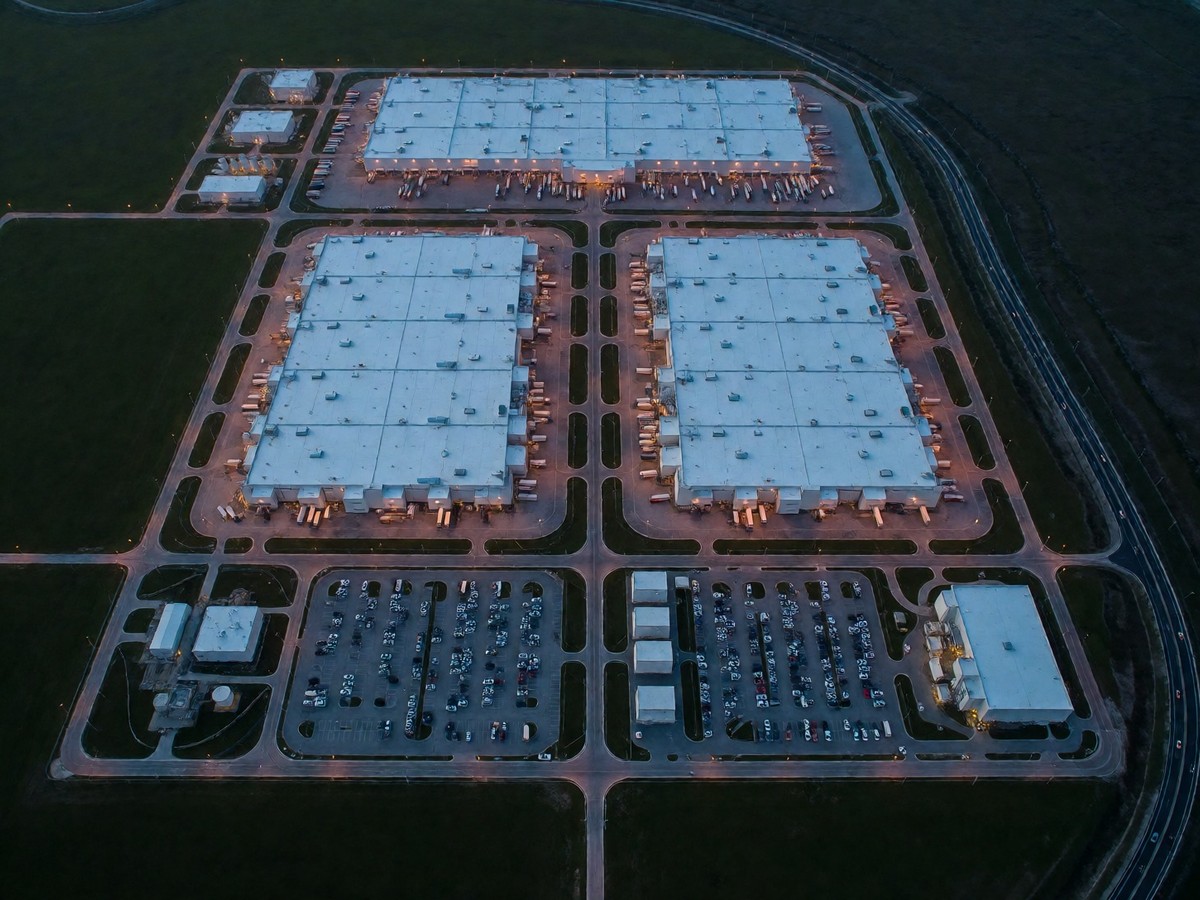
TSMC delivers 2nm mass production through its Hsinchu Baoshan and Kaohsiung facilities. The Baoshan plant, which serves as the mother fab for the N2 node, produces 25,000 wafers per month. TSMC targets a total capacity of 100,000 wafers per month by the end of 2026 to satisfy massive demand from the AI and mobile sectors. The N2 process provides a 15% performance boost at the same power level when compared to the 3nm generation. TSMC’s A16 node, which is an extension of the 2nm platform, provides an additional 8% to 10% speed increase at the same voltage compared to the N2P version. This A16 process also provides a 15% to 20% power reduction at the same clock frequency.
I see TSMC maintaining a clear lead in manufacturing maturity. The N2 yield rates have stabilized between 70% and 80%, providing a high volume of functional chips for customers. This stability allows TSMC to manage the massive chip demand from companies like Apple and NVIDIA. Apple has already reserved over 50% of the initial 2nm capacity for its A20 processors in the iPhone 18 series. NVIDIA also intends to use the A16 node to power its 2027 Feynman GPU architecture.
Intel 18A defect density and capacity
Intel produces 30,000 wafers per month through its Fab 52 site in Arizona and the D1X site in Oregon, providing enough volume to meet internal Panther Lake demand and satisfy external orders from Amazon. Intel 18A is a 1.8nm-class process that uses RibbonFET GAA architecture. Pat Gelsinger, the Intel CEO, states that the defect density for this process is below 0.4 defects per square centimeter. BlueFin Research Partners reports that the defect density is actually at the lower end of the 0.1 to 0.2 band. This level of defect density is similar to the maturity levels seen in TSMC’s N5 process before its mass production.
The 18A-P variant provides 9% more performance at the same power or 18% lower power at the same speed compared to the base 18A node. Intel’s 18A process is already used for internal products like the Panther Lake processor and the Clearwater Forest datacenter processor. External customers like Qualcomm and Amazon have also committed to the 18A node. NVIDIA has also expressed interest in 18A for specific AI inference chips. Intel expects to finish eight product tape-ins by the middle of 2025.
PowerVia and Super Power Rail implementations
The industry has entered the era of Backside Power Delivery (BSPDN), which changes how power reaches transistors. Intel uses a technology called PowerVia that utilizes Nano-Through Silicon Vias (nTSVs) to connect the power network to the back of the wafer. This implementation reduces IR drop, which is the voltage droop that occurs during electricity travel, from 7% to less than 1%. This change in power delivery increases transistor density by 30% and allows for more complex AI engines to fit in smaller footprints.
TSMC uses Super Power Rail (SPR) for its A16 node. This technology connects the power network directly to the source and drain of the transistors. This direct contact method is more difficult to manufacture than the nTSV approach used by Intel. TSMC projects that the A16 node provides a 15% to 20% power reduction compared to the N2P process. This power efficiency is necessary to handle the 1,000-watt power envelopes of future data center GPUs. You already know that advanced node economics depend on yield, so I will focus on the specific delta between TSMC and Intel.
AI accelerator customer commitments
The competition for AI silicon is split between TSMC’s high-yield capacity and Intel’s growing foundry presence. NVIDIA acts as a primary customer for TSMC, utilizing the 2nm and A16 nodes for its Rubin and Feynman architectures. AMD also uses TSMC’s 2nm process for its Instinct MI450 AI accelerators. These MI450 GPUs use the 2nm node to provide better performance, power efficiency, and transistor density.
Intel’s 18A node has also attracted significant AI interest. Xeon 6+ processors using the 18A node were selected as the host CPU for NVIDIA’s DGX Rubin. Microsoft and the U.S. Department of Defense have also confirmed plans to use Intel’s 18A production. While Intel has these commitments, NVIDIA has decided not to use Intel’s 18A for its foundry needs due to yield and performance concerns. This decision means NVIDIA will continue to rely on TSMC for much of its leading-edge manufacturing.
| Specification | TSMC N2 | TSMC A16 | Intel 18A |
|---|---|---|---|
| Transistor Architecture | Nanosheet GAAFET | Nanosheet GAAFET | RibbonFET GAA |
| Power Delivery | Frontside | Super Power Rail | PowerVia (nTSV) |
| Target Yield | 75% to 80% | Not yet specified | 55% to 60% |
| Monthly Capacity | 25,000 to 100,000 | 2H 2026 start | 30,000 |
| Key AI Customers | NVIDIA, AMD, Apple | NVIDIA, AMD | Amazon, NVIDIA |
Wafer pricing and manufacturing costs
The cost of advanced nodes creates a barrier for smaller designers. A single 2nm wafer from TSMC costs approximately $30,000. Apple’s 2nm wafers for the iPhone 18 cost roughly $27,000 each. NVIDIA’s backside power supply version of its chips costs over $30,000 per wafer. These high costs drive the high gross margins for TSMC, which reached 67.7% in the second quarter of 2026.
Intel’s financial position in the foundry market is different. Intel’s Foundry unit reported a loss of $2.1 billion in the second quarter of 2026 despite a 31% increase in revenue. Intel relies on a $5.0 billion NVIDIA equity investment and $8.9 billion in CHIPS Act funding to compete with TSMC. TSMC, however, self-funds its $52 billion to $56 billion 2026 capital expenditure program from its own cash flow. This difference in capital structure affects how each company manages its pricing and expansion.
Samsung 2nm yield failures
Samsung struggles to compete with TSMC in the 2nm market because of low yield rates. Reports show Samsung’s 2nm yield is around 40% to 45%, which is significantly lower than TSMC’s 75% to 80% range. Samsung’s trial production for its Exynos processor on the 2nm node shows a yield of only 30%. These low yields have caused Samsung to delay its 2nm production from late 2026 to the first quarter of 2027.
The yield gap leads to customer attrition for Samsung. Qualcomm continues to award its next-generation Snapdragon 8-series flagship orders to TSMC because of Samsung’s capacity and yield issues. Samsung is attempting to reach a 70% yield by mid-2027 to win back foundry customers. While Samsung secured a $16.4 billion order from Tesla for AI6 chips in July of last year, most external customers remain cautious. Will Intel’s 14A node eventually match TSMC’s A16 in yield stability?
Intel 18A versus TSMC A16 for AI workloads
Intel and TSMC compete for the dominance of the AI data center. Intel’s 18A node provides an advantage in energy efficiency for specific high-performance computing scenarios because it was a pioneer in backside power delivery. Intel’s 18A-P variant offers 18% lower power at the same speed compared to the base node. This makes it a strong candidate for AI inference and edge computing.
TSMC’s A16 node focuses on extreme performance for massive AI training models. The Super Power Rail method is designed to handle the high amperage requirements of large-scale language models. TSMC maintains its leadership through its massive scale and deep partnerships with AMD and NVIDIA. Intel’s realistic win for 2026 is to prove 18A yield maturity and secure secondary packaging orders. I recommend TSMC for core AI exposure because its 70% to 80% yield provides a reliable supply of high-performance silicon. Intel 18A remains a high-risk, high-reward play for those betting on US-based manufacturing.