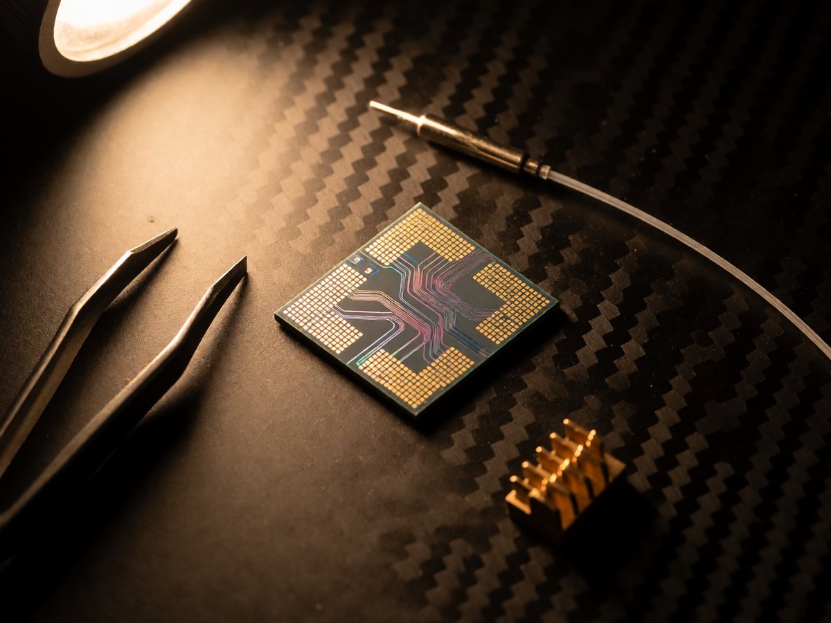
Marvell agreed to acquire Celestial AI in a definitive deal valued at $3.25 billion upfront. The transaction includes $1 billion in cash and 27.2 million shares valued at $2.25 billion based on the 10-day volume-weighted average price. Additional equity worth up to $2.25 billion depends on revenue milestones. One third of the earn-out triggers if Celestial AI hits $500 million in cumulative revenue by the end of fiscal 2029. The full earn-out requires $2 billion in cumulative revenue by that same date. Marvell expects the business to begin contributing revenue in the second half of fiscal 2028. It expects a $500 million annualized run rate by the fourth quarter of fiscal 2028 and $1 billion by the fourth quarter of fiscal 2029. This acquisition targets the 16 Tbps Photonic Fabric optical interconnect platform. Founded in 2020, Celestial AI builds these 16 Tbps chiplets to connect XPUs across packages, systems, and racks.
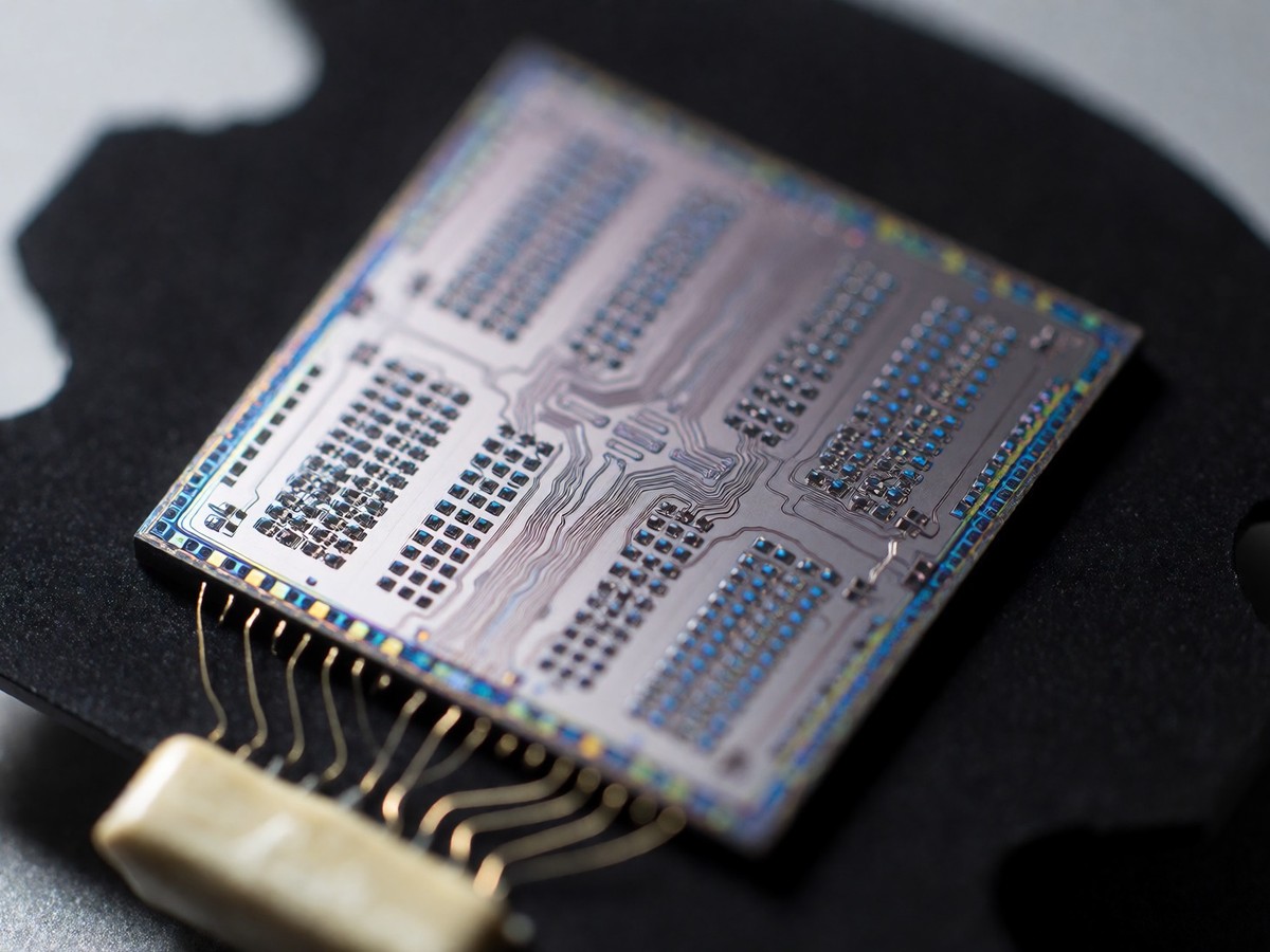
The Photonic Fabric integrates electrical and optical components in a compact form factor. These chiplets co-package directly with XPUs and scale-up switches. This arrangement allows optical links to originate from the center of the die. This design frees die-edge area for additional HBM capacity. Because the Photonic Fabric integrates electro-absorption modulators directly into 2.5D interposers and bridges using TSMC CoWoS, it maintains stability during the extreme thermal excursions of 500W to 900W GPUs that operate adjacent to multi-kilowatt XPUs. The platform uses electro-absorption modulators instead of ring modulators to maintain stability during temperature swings above 85 degrees Celsius. It also survives rapid temperature excursions of 200 degrees Celsius per second.
Comparing the interconnects
I find the efficiency of the Photonic Fabric compelling. The custom analog-only SerDes consumes 2.4 pJ/bit for electronics and 0.7 pJ/bit for lasers. This yields 2x better efficiency than DSP-based designs. The platform delivers latencies of 100 ns for NIC-to-NIC paths and under 200 ns for chip-to-memory transactions. The Optical Multi-Chip Interconnect Bridge (OMIB) embeds photonics into package bridges to support in-die optical connections. This structure potentially drops memory transactions directly into cache and reduces on-die travel latency.
| Metric | Celestial AI Photonic Fabric | NVIDIA NVLink-C2C (GH200) |
|---|---|---|
| Chiplet Bandwidth | 16 Tbps | 900 GB/s per direction |
| Power (Electronics) | 2.4 pJ/bit | 6x efficiency vs PCIe Gen 6 |
| Latency (Chip-to-memory) | <200 ns | Sub-microsecond |
NVIDIA uses NVLink-C2C to connect GPUs and CPUs in integrated products. In the GH200 Superchip, each GPU tile exposes between 18 and 22 NVLink-C2C links. These links reach an aggregate one-way bandwidth of 900 GB/s. Multi-GPU configurations reach 1.2 TB/s bidirectional bandwidth. NVLink-C2C provides 6x more energy efficiency and 3.5x more area efficiency than a PCIe Gen 6 PHY on NVIDIA chips. The technology supports Arm’s AMBA CHI or CXL industry standard protocols for interoperability.
Scaling limits and market realities
The industry faces a hard reality regarding copper interconnects. Signal loss and power consumption drive the move toward optical solutions. TrendForce predicts the market for co-packaged optics and near-packaged optics will grow from $100 million in 2025 to over $39 billion by 2030. You probably know the basics of HBM2e, but the interconnect dictates the actual scale of the AI factory.
The A100 SXM4 module mounts on NVIDIA HGX baseboards and pulls 400W. The PCIe variant draws 300W. The SXM4 variant delivers 2,039 GB/s of memory bandwidth compared to 1,935 GB/s for the PCIe version. The SXM4’s NVLink provides 600 GB/s of bi-directional bandwidth. On an HGX A100 baseboard, the aggregate GPU-to-GPU bandwidth is 2.4 TB/s for a 4-GPU node and 4.8 TB/s for an 8-GPU node. In a memory-bound HPL-AI benchmark, a 4-GPU A100 SXM4 system delivered 485 TFLOPS, while a 4-GPU A100 PCIe system managed 110 TFLOPS. If you use the PCIe version, you are limited to 64 GB/s per x16 link. The SXM4’s higher power headroom and cooling allow it to sustain higher real-world throughput under long, heavy loads.
The complexity of manufacturing co-packaged optics remains a massive hurdle for large-scale adoption. Yield issues and fiber-connector standardization persist as significant blockers. I would skip the dream of immediate universal adoption if I were planning a cluster for next month. Will the industry manage the supply chain constraints for InP substrates and lasers before the demand for scale-up architectures peaks?