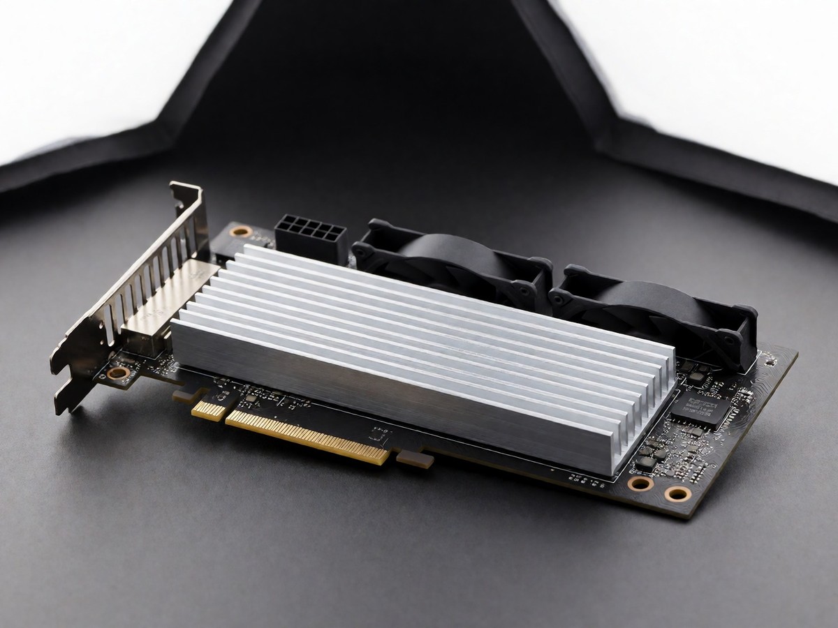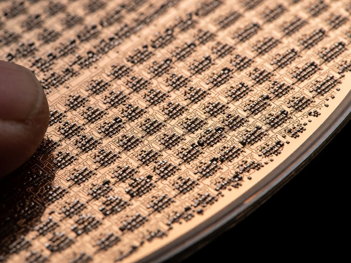
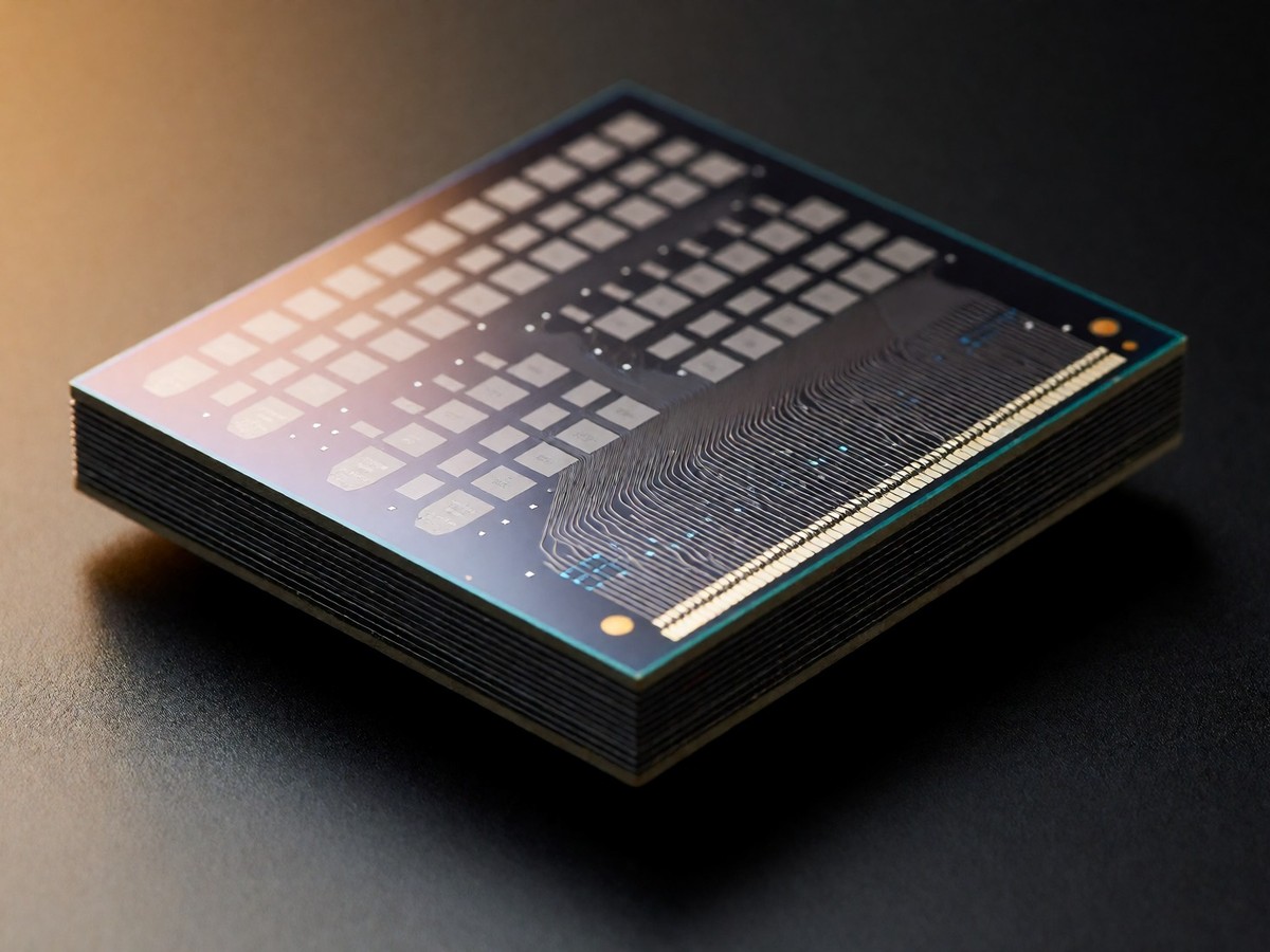
Lightmatter’s Passage platform uses silicon photonics to replace copper links between AI accelerators and switches. This technology provides 114 Tbps of optical bandwidth via the Passage M1000. The M1000 is a 3D photonic interposer that sits beneath the processor to allow edgeless I/O. This design reduces power consumption by 3.5 times compared to legacy copper. The product line includes the Passage L200, which is a 3D co-packaged optics solution, and the Passage L20, which functions as a near-packaged optics module. The L20 provides 6.4 Tbps of bandwidth in each direction and has a 30 W maximum TDP. It uses standard 224G-class electrical interfaces. The M1000 remains a reference platform without confirmed customer deployments. The M1000 is an 8-tile 3D active interposer with 34 integrated chiplets and 1,024 electrical SerDes. It uses 56 Gbps NRZ modulation and 8 wavelength WDM transmission on waveguides and fibers. The device has 256 edge-attached optical fibers that provide 448 Gbps of bandwidth per fiber. This 4,000 square millimeter platform uses a reconfigurable waveguide network. It delivers 1.5 kW of power delivery in an integrated advanced package.
Integration with NVIDIA NVLink Fusion
Lightmatter joined the NVIDIA NVLink Fusion ecosystem to enable custom XPUs to connect with NVIDIA switch silicon. This integration allows specialized accelerators to work within the NVIDIA rack architecture. The Passage platform addresses the shoreline problem where electrical input/output connections are restricted to the edges of a chip. By using 3D integration, Lightmatter allows SerDes to sit anywhere on the die. You already know that copper signals degrade over distance and create heat in large clusters. Lightmatter’s partnership with Qualcomm uses 112G PAM4 SerDes to enable 1.6 Tbps of bandwidth per fiber for the Passage EVK100. This approach helps bridge the gap between custom silicon and established networking stacks. By adapting Lightmatter’s bi-directional optical link architecture for NVIDIA’s optical and electrical technology, Lightmatter creates a unified platform for semi-custom AI factories while reducing fiber and connector requirements by 50%. The integration of Passage CPO solutions with NVIDIA’s NVLink Fusion architecture combines the industry’s most advanced AI platform and the world’s leading interconnect. This integration supports the deployment of the next generation of frontier AI models. The NVLink Fusion ecosystem provides partners with the ability to integrate custom silicon with NVIDIA’s deep ecosystem of NVLink, advanced packaging, rack-scale systems, and networking technologies.
Market Scale and Technical Specifications
The market for optical interconnects is moving from technological novelty to a focus on manufacturing scale. Lightmatter’s Guide platform provides a laser light source to support these photonic engines. This module can feed 204.8 Tbps of CPO switching in a 1RU tray. The market is currently split between pluggable optics and co-packaged optics. While pluggable transceivers meet immediate demand, co-packaged optics like the L200 aim for higher density. Lightmatter provides the most complete photonic interconnect stack outside a public chipmaker. The Passage M1000 utilizes the GF Fotonix silicon photonics platform with Amkor packaging to create a multi-reticle active photonic interposer. The L200 family uses chip-on-wafer bonding to stack an electronic IC on the photonic chip. The L200 provides 32 Tbps of bidirectional bandwidth, while the L200X delivers 64 Tbps. These products aim for up to 8x faster AI model training. The optical interconnect and transceiver markets project to exceed $80 billion by the early 2030s. Ayar Labs delivers the TeraPHY chiplet with 8 Tbps of bandwidth per chiplet. Celestial AI delivers the Photonic Fabric with 14.4 Tbps of bandwidth. Lightmatter maintains a valuation of $4.4 billion as of October 2024 and employs approximately 165 people. The L20 CPX is a bidirectional module that uses two wavelengths per fiber. This design halves fiber management needs compared to standard DR optics. For a 512-GPU pod, this can reduce fiber strands from 130,000 to 65,000. This architecture provides a 15% reduction in scale-up interconnect cost for such pods. Will the industry move to mass-produced co-packaged optics by 2028?
| Product | Type | Bandwidth | Availability |
|---|---|---|---|
| Passage M1000 | Photonic Interposer | 114 Tbps | Summer 2025 (Sampling) |
| Passage L200 | Co-packaged Optics | 32 Tbps | 2026 |
| Passage L200X | Co-packaged Optics | 64 Tbps | 2026 |
| Passage L20 | Near-packaged Optics | 6.4 Tbps | Late 2026 (Sampling) |