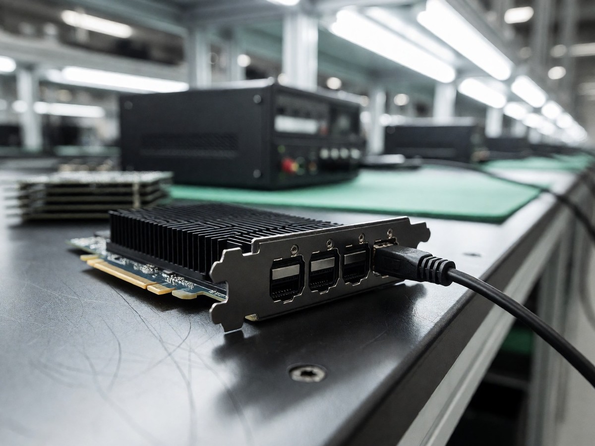

I see the industry hitting the physical limits of copper wires. Lightmatter’s Passage platform uses 3D-stacked silicon photonics to place AI accelerators directly on a photonic layer. This architecture provides 114 Terabits per second (Tbps) aggregate bandwidth with a density of 1.4 Tbps/mm2. The system uses the Guide light engine, which integrates up to 64 laser wavelengths on one platform. This design achieves sub-2 nanosecond hop times between data entry and exit points. You should ignore the hype about pluggable transceivers because Passage bypasses the shoreline bottleneck entirely. However, lasers remain sensitive to heat, so the 3D stacking introduces difficult thermal management requirements. Passage consists of a flat, rectangular piece of silicon made from an entire wafer. Up to tens of chiplets sit atop this wafer. The platform uses compact, embedded waveguides to move light. These waveguides are so dense that 40 of them fit in the space of a single optical fiber. This configuration delivers a 1,600 Gbps Passage platform when built with Qualcomm. The design also supports 400Gbps Tx and 400Gbps Rx using a DWDM bi-directional link architecture with 16 wavelengths per fiber. The system works with 8-wavelength, 4+4 band interleaving to ensure interoperability. Lightmatter also provides the Envise 4S server, which uses 16 custom chips with 256 RISC cores each. This server completes three times more computing instructions per second than the NVIDIA DGX-A100. The Envise 4S includes two off-the-shelf AMD processors and three terabytes of onboard flash memory.
Scaling through Co-Packaged Optics
Lightmatter partners with Global Unichip (GUC) to commercialize Co-Packaged Optics (CPO) solutions. GUC provides advanced ASIC design and packaging using TSMC’s CoWoS and SoIC technologies. They bond electronic integrated circuits with photonic integrated circuits.
| Feature | Passage M1000 Specification |
|---|---|
| Aggregate Bandwidth | 114 Tbps |
| Bandwidth Density | 1.4 Tbps/mm2 |
| Wavelength Capacity | Up to 64 wavelengths |
| Hop Time | < 2 nanoseconds |
| Power Usage | 1/5 of traditional interconnects |
| Waveguide Density | 40 waveguides per optical fiber space |
By integrating optical engines directly onto the silicon package, Lightmatter and GUC enable a new generation of AI factories that operate with extreme efficiency while reducing the power budget spent moving data between chips instead of processing it. A technical collaboration with Cadence adds high-speed SerDes IP and Universal Chiplet Interconnect Express (UCIe) IP to the stack. GUC also provides HBM3 PHY and controller designs running at 8.4 Gbps. These efforts target the energy and performance limits of legacy signaling. The partnership addresses thermal, mechanical, and signal integrity challenges. Analysts expect the market for integrated optical-compute platforms to reach $103.26 billion by 2035. This work helps commoditize the optical backbone of the chiplet era for hyperscale customers.
A fight for AI dominance
NVIDIA and AMD control the market for electrical interconnects like NVLink and Infinity Fabric. AMD’s Infinity Fabric has a maximum theoretical bandwidth of 800 Gbps, while Passage offers 96 TBps of bandwidth to each die. Lightmatter’s valuation sits above $4.4 billion after raising $850 million total. Ayar Labs also competes in this space with its TeraPHY module and $370 million in funding. Ayar Labs uses SuperNova remote light technology to transmit data between computer chips via light. Its recent $155 million Series D round was led by Advent Global Opportunities and Light Street Capital. This round included participation from NVIDIA, AMD, Intel, and GlobalFoundries. VentureTechAlliance also participated through its strategic partnership with TSMC. Ayar Labs’ TeraPHY module is an in-package I/O chiplet that integrates with system-on-chip packages to improve the profitability metrics of AI applications. Xscape Photonics raised $44 million in October, while Lightium AG closed a $7 million seed round in September. The industry faces a need for technologies that eliminate bottlenecks as AI infrastructure spending reaches $1 trillion over the next decade, according to Goldman Sachs. Cloud providers like Amazon, Microsoft, and Google design custom chips to reduce dependency on external vendors and improve performance. Amazon’s custom chips, such as Inferentia, enable faster and more cost-effective AI processing. Microsoft’s custom hardware helps bolster cloud computing and drive AI research. Google works toward carbon-free energy by 2030. Can these specialized optical solutions actually displace the established electrical dominance of NVIDIA and AMD in massive data centers?