The 3D photonic architecture
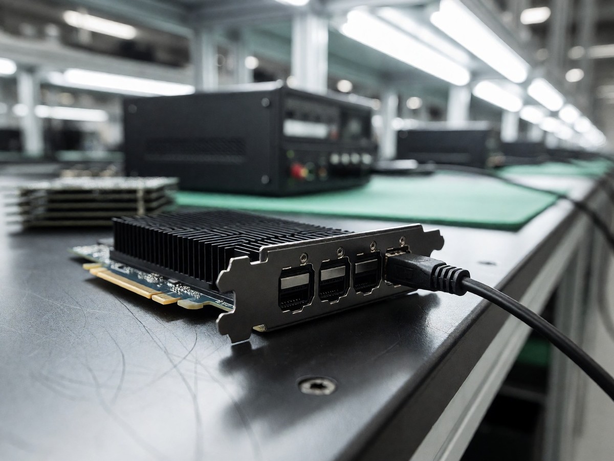
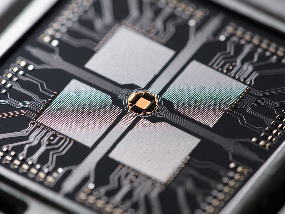
Lightmatter addresses the AI data center bandwidth bottleneck using the Passage platform. Traditional electrical and optical interconnects rely on the chip perimeter, or shoreline, for data movement. As chip area scales, this perimeter-based I/O creates a hard ceiling on aggregate bandwidth. Passage uses 3D vertical integration to place I/O across the entire die area instead of just the edges. This architecture enables bandwidth density to scale with the die area rather than just the perimeter.
| Product | Max Bandwidth | Key Feature |
|---|---|---|
| Passage M1000 | 114 Tbps | 4,000 mm2 interposer |
| Passage L200 | 32 Tbps | 16 wavelength division multiplexing |
| Passage L200X | 64 Tbps | 106/112 Gbps PAM4 |
| Passage L20 | 12.8 Tbps | Near-package/On-board |
The Passage M1000 provides 114 terabits per second of total bidirectional bandwidth and 1,024 high-speed SerDes lanes through a 4,000 square millimeter photonic interposer that connects up to 34 chiplets across the die. This platform connects massive amounts of data. The L200 and L200X models provide 32 and 64 terabits per second of aggregate bandwidth respectively. These L-series modules use 16 wavelength division multiplexing per waveguide to support 800 Gbps or 1.6 Tbps per fiber. The L20 configuration allows for near-packaged optics on the PCB or on-board optics with a retimer for extreme reach. These L200 products use 320 optically-optimized multi-rate SerDes and a 32 Gbps UCIe die-to-die interface. They arrive in 2026 to support next-generation XPUs and switches. This capability addresses the reality that switch and XPU bandwidths scale faster than electrical signaling can follow.
Ayar Labs holds the commercial lead, while Lightmatter holds the technical ceiling
Ayar Labs and Lightmatter lead the optical interconnect market, yet they follow different paths. Ayar Labs uses TeraPHY optical engine chiplets at the chip interface to minimize changes for existing chip designers. Lightmatter uses a full-surface photonic layer beneath the entire chip surface. Lightmatter’s full-surface approach increases manufacturing and integration complexity compared to edge-only chiplet solutions. Ayar Labs reported a valuation above $5 billion in 2026, while Lightmatter’s last disclosed valuation was $4.4 billion in 2024. Ayar Labs also raised $150 million in September 2026, bringing its 2026 primary funding to $650 million.
Ayar Labs targets an easier integration path for customers by using standard packaging flows and foundry processes. Their TeraPHY engine delivers over 8 terabits per second of bidirectional bandwidth per device. Lightmatter targets higher peak performance by replacing traditional perimeter I/O with edgeless connectivity. Ayar Labs aims for volume-production qualification by the end of 2027, with customer ramps starting in 2028. Lightmatter plans for low-volume co-packaged shipments in 2027 and high-volume deployment in 2028. Which company will secure the first large-scale hyperscaler production contract?
The competitive field contains several other active players. Ranovus maintains a third-place position with its 6.4 Tbps ODIN engine, its Jabil production route, and its work on a DARPA-backed Cerebras project. Avicena began shipping 1 Tbps microLED evaluation kits in August 2026, which provide double the bandwidth of its first kit. Salience Labs raised a $125 million Series B in October 2026 and demonstrated a 64-port optical circuit switch in September. Ayar Labs has strategically backed partners including AMD, Intel, MediaTek, and Nvidia.
The ecosystem for AI scale-up
The industry is moving toward co-packaged optics to manage power and density. Lightmatter partnered with GUC to combine Passage with advanced ASIC design services. This collaboration aims to solve architectural, thermal, and signal integrity challenges for hyperscale customers. Lightmatter also joined the NVIDIA NVLink Fusion ecosystem in June 2026 to provide products compatible with NVIDIA technologies. The company is also participating in an Open Compute Project initiative with partners including Dell Technologies, Flex, Foxconn Interconnect Technology, Hyve Solutions, Keysight, Qualcomm Technologies, and Quanta Cloud Technology.
Lightmatter manages a broad manufacturing network including Intel, GlobalFoundries, Tower, Amkor, and ASE. Flex uses the Lightmatter switch tray to validate its own photonics production line. The company is currently evaluating its Passage engines with major hyperscalers and chip designers. You should monitor if the 2027 shipment targets for the M1000 interposer meet the demand of frontier AI models. Lightmatter provides a complete, vertically integrated solution including Guide light engines and Idiom software. The Passage M1000 interposer reaches 114 Tbps from a single package.
The current AI training landscape creates a gap between compute growth and interconnect speed. AI model parameters grew 240 times over three years, but interconnect bandwidth improved only twofold. Modern AI training clusters depend on the speed of data movement between thousands of chips. While NVIDIA expands GPU clusters and Cerebras uses wafer-scale engines, Lightmatter attempts to collapse datacenter-level communication into a single superchip. This requires bypassing the physical limits of copper and the shoreline constraints of traditional silicon. NVIDIA’s next-generation Blackwell architecture explicitly requires 1.6 Tbit/s optical interconnect requirements to support its demands.