Thermal Mismatch and Design Redesign
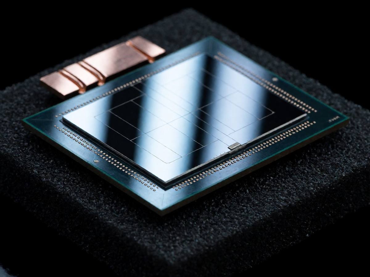
The coefficient of thermal expansion mismatch between the GPU chiplets, the silicon bridges, the RDL interposer, and the motherboard substrate causes warping and complete system failure for the entire Silicon in Package, requiring an immediate design overhaul. This mismatch forces NVIDIA to redesign the top global routing metal layers and bumps of the GPU silicon to improve yields. This technical instability makes the firm seem less reliable to its primary customers. Large shipments of Blackwell products face delays of three months or more. Google ordered 400,000 GB200 chips in a deal exceeding $10 billion, while Meta and Microsoft face uncertain delivery timelines for their massive investments. The complex GB200 NVL72 rack contains 1.2 million components and weighs nearly 2 tons. These systems require the precise placement of bridge dies to maintain a 10 TB/s interconnect. The GB200 utilizes fifth-generation NVLink, providing 14 times the bandwidth of PCIe 5.0. Microsoft’s intention to have GB200 GPUs ready for OpenAI by the first quarter of 2025 is now in doubt. NVIDIA also faces an investigation by the US Department of Justice regarding alleged anti-competitive practices. This mismatch is a primary cause of the multi-month delay.
Packaging Bottlenecks and Memory Shortages
TSMC capacity for CoWoS-L falls short of the demand for Blackwell. The company builds a new facility in Chiayi and converts AP3 capacity, but the ramp remains lumpy. NVIDIA focuses its limited CoWoS-L allocation on GB200 NVL72 and NVL36 rack systems. These systems require liquid cooling due to a 140 kW thermal design power per rack. High Bandwidth Memory (HBM3e) production also limits Blackwell shipments. SK Hynix holds 50% of HBM revenue, Samsung holds 33%, and Micron holds the remaining market share. Higher die stacks and tighter tolerances in HBM3e lead to a 5% to 8% loss for every additional die added beyond an 8-layer stack. OSAT companies like Powertech and KYEC expanded capital expenditures to enhance advanced packaging. TSMC is building a new fab, AP6, for CoWoS-L. The Chiayi facility will occupy 20 hectares, with the first facility covering 12 hectares, and is expected to create 3,000 jobs. The demand for advanced packaging for AI chips continues to outstrip supply. The capacity gap for CoWoS is projected to narrow from 20% to 10% by the end of 2026.
| Feature | NVIDIA Blackwell B200 | NVIDIA H100 |
|---|---|---|
| Memory Capacity | 192 GB HBM3e | 80 GB HBM3 |
| Memory Bandwidth | 2.4x H100 | Baseline |
| FP16/BF16 Throughput | 2x H100 | Baseline |
Power Demands and the B200A Pivot
NVIDIA introduces the B200A to bypass the CoWoS-L bottleneck. The B200A uses a monolithic B102 die that fits on CoWoS-S or other 2.5D packaging from Amkor or ASE. This version uses less memory bandwidth than the H200 but targets mid-range AI systems. The B200A replaces the B100 and B200 chips for HGX 8-GPU form factors. This chip provides up to 144GB of HBM3E and 4 TB/s of memory bandwidth. The B200 provides 2.4x the memory bandwidth and double the FP16/BF16 throughput of the H100. An 8x B200 cluster draws 4.8 kW for GPUs and 6.5 to 7 kW total. This cluster trains computer vision models 57% faster than an 8x H100 setup. The B200A Ultra features a new MGX NVL36 form factor and 288GB of HBM3E with a 50% increase in FLOPS. AMD competes with the MI350X using CoWoS-S. You know the struggle of scaling power density, so the 140 kW requirement for the GB200 NVL72 should not come as a surprise. To manage such heat, manufacturers use sidecar CDUs that dissipate between 60 kW and 80 kW. The Blackwell architecture is a technical disaster that threatens NVIDIA’s dominance. Will the redesigned B200A successfully stabilize the supply chain for mid-range AI workloads?