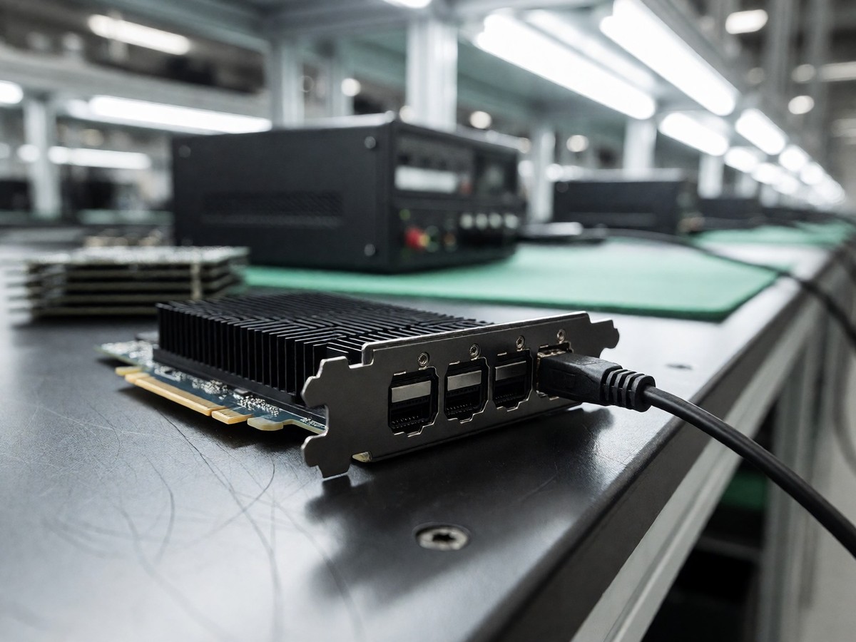

Lightmatter secured $400 million in Series D funding to expand production of its photonic chips, which use light instead of electricity for AI computing. This investment, led by new investors advised by T. Rowe Price Associates, brings the company’s total capital raised to $850 million and sets its valuation at $4.4 billion. The company plans to use these funds to deploy its Passage technology in partner data centers. Lightmatter’s Passage technology uses 3D-stacked photonics chips for data movement to increase AI cluster bandwidth and performance while lowering power consumption.
Traditional electrical interconnects struggle to meet the high-bandwidth, low-latency requirements of AI workloads as training clusters exceed 100,000 XPUs. Current electrical SerDes technology faces limits in bandwidth and reach because chips lack sufficient edge space for I/O. Model parameters grew 240x in three years, while cluster sizes grew 10x, but interconnect bandwidth only improved 2x. This widening gap makes next-generation AI training economically difficult. Lightmatter’s Passage M1000 3D photonic interposer serves as a reference platform for connecting GPUs, TPUs, and data center switches in large AI model training clusters.
| Specification | Passage M1000 / Photonic Platform Detail |
|---|---|
| Deployment Target | 100,000+ GPU clusters |
| Aggregated Bandwidth | 114 Tbps across 4,000 mm2 footprint |
| Signaling Type | 112G PAM4 |
| Scaling Capability | 32 to 64 Tbps via co-packaged optics |
| Bidirectional Link | 800 Gbps per fiber at 2.6 pJ/bit |
| Light Source Technology | Guide VLSP technology |
Breaking the copper backplane limit
The Passage M1000 addresses the physical limitations of electrical I/O by increasing the XPU shoreline to support more memory. Because the technology delivers I/O in 3D, it overcomes the bottlenecks that restrict AI performance scaling. Lightmatter’s technology integrates with the NVIDIA NVLink Fusion ecosystem to provide high bandwidth and energy efficiency for hyperscalers. The company’s Guide light engine supports hundreds of lasers and photonics components on a single chip to power co-packaged optics. This Guide platform uses Very Large Scale Photonics technology to provide a stable, replaceable, and thermally isolated light source.
Lightmatter’s approach uses micro-ring modulators (MRMs) which are compact and power-efficient. These devices function as wavelength-selective filters that couple light from a bus waveguide into a ring. To maintain stability, Lightmatter engineers must manage thermal transients of 800°C/sec and coordinate complex sequencing for multi-wavelength operation. The company has developed expertise in MRM control and firmware validation over eight years across multiple generations of silicon. In 2025, Lightmatter demonstrated 800 Gbps on a single fiber with a 16-wavelength, 53.125 Gbaud NRZ, bidirectional link.
The physical density of fiber plants creates a binding constraint as clusters scale from tens of thousands to hundreds of thousands of accelerators. Lightmatter uses bidirectional fiber to double the number of logical connections a fiber plant supports by running transmit and receive functions in the same fiber using separate wavelength bands. Dense Wavelength-Division Multiplexing (DWDM) further maximizes bandwidth per link. The OCI MSA specification defines Group A wavelengths (1308 – 1315 nm) and Group B wavelengths (1328 – 1335 nm) to facilitate this bidirectional operation.
Hardware deployment and NVIDIA Blackwell constraints
NVIDIA reported design flaws in the processor die that connects two Blackwell GPUs on a GB200, which delayed the rollout of its Blackwell GPU family by three months or more. This production issue, discovered by manufacturer TSMC, forces NVIDIA to adjust the design and run new production tests. These delays impact the plans of hyperscalers like Google, Meta, and Microsoft to operate new AI data centers. While NVIDIA considers producing a version with only one Blackwell GPU to speed delivery, the supply of large clusters remains affected.
Lightmatter addresses these scaling needs through its partnership with Global Unichip Corp. (GUC). This collaboration combines GUC’s ASIC design and packaging with Lightmatter’s Passage 3D Co-Packaged Optics (CPO) solutions. The integrated solution uses GUC’s advanced node chiplet and packaging workflows to overcome the physical I/O limits of the chip. This scalability helps extend the scale-up domain of AI clusters across multiple racks.
The deployment of these photonic systems requires significant capital and specialized hardware. Lightmatter’s leadership team includes former Google TPU lead Richard Ho and former Intel datacenter chip packaging lead Ritesh Jain. The company holds over 150 patents worldwide and employs more than 200 people. The massive power consumption and heat loads from generative AI systems drive the need for these photonic solutions. Lightmatter’s technology aims to reduce AI training power by over 90%. Will the industry adopt these 3D photonic interconnects fast enough to keep pace with the rapid growth of trillion-parameter models?